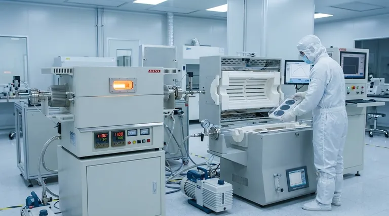
In the electronics and semiconductor industries, vacuum furnaces are indispensable tools for manufacturing high-performance components. They are used for critical processes like doping and annealing silicon wafers, sintering ceramic substrates, and diffusion bonding circuits, where an ultra-clean, controlled environment is non-negotiable for ensuring device reliability and performance.
The core function of a vacuum furnace is not just to provide heat, but to create a chemically inert environment. By removing reactive gases like oxygen, it prevents contamination and oxidation, allowing for the fabrication of materials with the precise atomic-level purity and structural integrity that modern electronics demand.
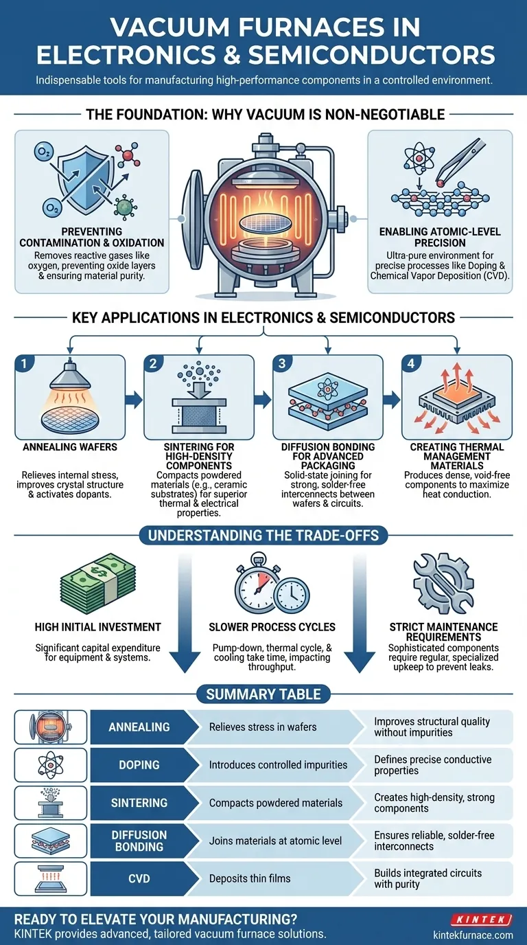
The Foundation: Why a Vacuum is Non-Negotiable
The extreme sensitivity of semiconductor materials means that even microscopic impurities or oxides can cause a device to fail. A vacuum furnace directly addresses this challenge by removing the atmospheric gases that would otherwise react with materials at high processing temperatures.
Preventing Contamination and Oxidation
At the high temperatures required for fabrication, materials like silicon are highly reactive. Any exposure to oxygen or other atmospheric contaminants would create unwanted oxide layers, altering the material's electrical properties.
A vacuum environment removes these reactive agents, creating a pristine canvas for processes like doping or film deposition. This ensures that the final component has the exact chemical makeup intended.
Enabling Atomic-Level Precision
Processes like doping involve intentionally introducing controlled impurities into a silicon wafer to define its conductive properties. Chemical Vapor Deposition (CVD) involves depositing exceptionally thin films, like silicon nitride or polysilicon, to build integrated circuits.
Both processes require an ultra-pure environment so that only the desired atoms are added. A vacuum furnace provides this essential clean slate, preventing stray molecules from interfering with the atomic-scale construction.
Key Applications in Electronics and Semiconductors
The controlled environment of a vacuum furnace is leveraged for several mission-critical manufacturing steps, from creating the base wafer to packaging the final component.
Annealing Wafers
Annealing is a heat treatment process used to relieve internal stresses within the silicon crystal lattice and to activate dopants. Performing this in a vacuum ensures that the process improves the material's structural quality without introducing new surface impurities or defects.
Sintering for High-Density Components
Sintering is the process of compacting powdered materials into a solid mass using heat and pressure. In electronics, vacuum hot presses are used to create high-density ceramic substrates for microchips.
The vacuum is critical for removing trapped gases between the powder particles. This results in a final component that is denser, stronger, and has superior thermal and electrical properties.
Diffusion Bonding for Advanced Packaging
Diffusion bonding is a solid-state joining technique that bonds materials together at an atomic level without melting or using solder. It is used to join semiconductor wafers and circuits.
For this bond to form, the surfaces must be perfectly clean. A vacuum furnace removes any surface contaminants, allowing direct, high-integrity bonds that are essential for reliability in high-performance electronics.
Creating Thermal Management Materials
High-power electronics generate significant heat. Vacuum furnaces are used to produce thermal management components like heat spreaders and insulators. The vacuum process ensures these materials are highly dense and free of voids, maximizing their ability to conduct heat away from sensitive circuits.
Understanding the Trade-offs
While essential, vacuum furnace technology comes with inherent complexities and costs that must be considered.
High Initial Investment
Vacuum furnaces, along with their associated pumps, control systems, and instrumentation, represent a significant capital expenditure compared to standard atmospheric furnaces.
Slower Process Cycles
Achieving a high vacuum (pump-down), running the thermal cycle, and cooling the components in a controlled manner takes significantly more time than atmospheric processing. This can impact overall manufacturing throughput.
Strict Maintenance Requirements
The seals, pumps, and sensors that maintain the vacuum are sophisticated components that require regular, specialized maintenance. Any leak can compromise the entire process, making vigilant upkeep critical.
How to Apply This to Your Goal
The specific vacuum process you need depends entirely on your end product and the material properties you aim to achieve.
- If your primary focus is fabricating integrated circuits: Your key processes will be vacuum annealing, doping, and CVD for depositing pure, uniform films onto silicon wafers.
- If your primary focus is advanced component packaging: You will rely on diffusion bonding for strong, solder-free interconnects and vacuum sintering for high-density, reliable substrates.
- If your primary focus is creating passive or structural components: Vacuum hot pressing and sintering are essential for producing materials like heat spreaders and ceramic insulators with optimal density and thermal properties.
Ultimately, mastering the controlled environment of a vacuum furnace is the key to unlocking the performance, purity, and reliability required by the modern electronics landscape.
Summary Table:
| Process | Key Function | Benefit in Electronics/Semiconductors |
|---|---|---|
| Annealing | Relieves stress in silicon wafers | Improves structural quality without impurities |
| Doping | Introduces controlled impurities | Defines precise conductive properties |
| Sintering | Compacts powdered materials | Creates high-density, strong components |
| Diffusion Bonding | Joins materials at atomic level | Ensures reliable, solder-free interconnects |
| CVD | Deposits thin films | Builds integrated circuits with purity |
Ready to elevate your electronics and semiconductor manufacturing with precision vacuum furnace solutions? At KINTEK, we leverage exceptional R&D and in-house manufacturing to provide advanced high-temperature furnaces, including Muffle, Tube, Rotary, Vacuum & Atmosphere Furnaces, and CVD/PECVD Systems. Our strong deep customization capability ensures we can precisely meet your unique experimental and production needs, delivering enhanced purity, reliability, and performance for your components. Contact us today to discuss how our tailored solutions can drive your success!
Visual Guide
Related Products
- Vacuum Hot Press Furnace Machine Heated Vacuum Press Tube Furnace
- Vacuum Hot Press Furnace Machine Heated Vacuum Press
- 600T Vacuum Induction Hot Press Vacuum Heat Treat and Sintering Furnace
- 2200 ℃ Tungsten Vacuum Heat Treat and Sintering Furnace
- Vacuum Heat Treat Sintering Furnace with Pressure for Vacuum Sintering
People Also Ask
- What control features does a vacuum hot press furnace offer? Precision Control for Advanced Materials Processing
- What is a vacuum hot press furnace? Unlock Superior Material Performance
- How does a vacuum hot press furnace promote densification in the manufacturing of graphite flake/copper composites? Achieve Superior Composite Materials
- What temperature control features do vacuum hot press furnaces have? Achieve Precision in High-Temp Material Processing
- What safety features are incorporated in vacuum hot press furnaces? Ensure Operator and Equipment Protection


