In the semiconductor industry, vacuum furnaces are indispensable for critical manufacturing steps such as annealing, doping, and thin-film deposition. These processes require an ultra-clean, tightly controlled environment to fabricate integrated circuits, and the furnace's vacuum ensures that silicon wafers are not compromised by atmospheric contamination or oxidation, which would be catastrophic to device function.
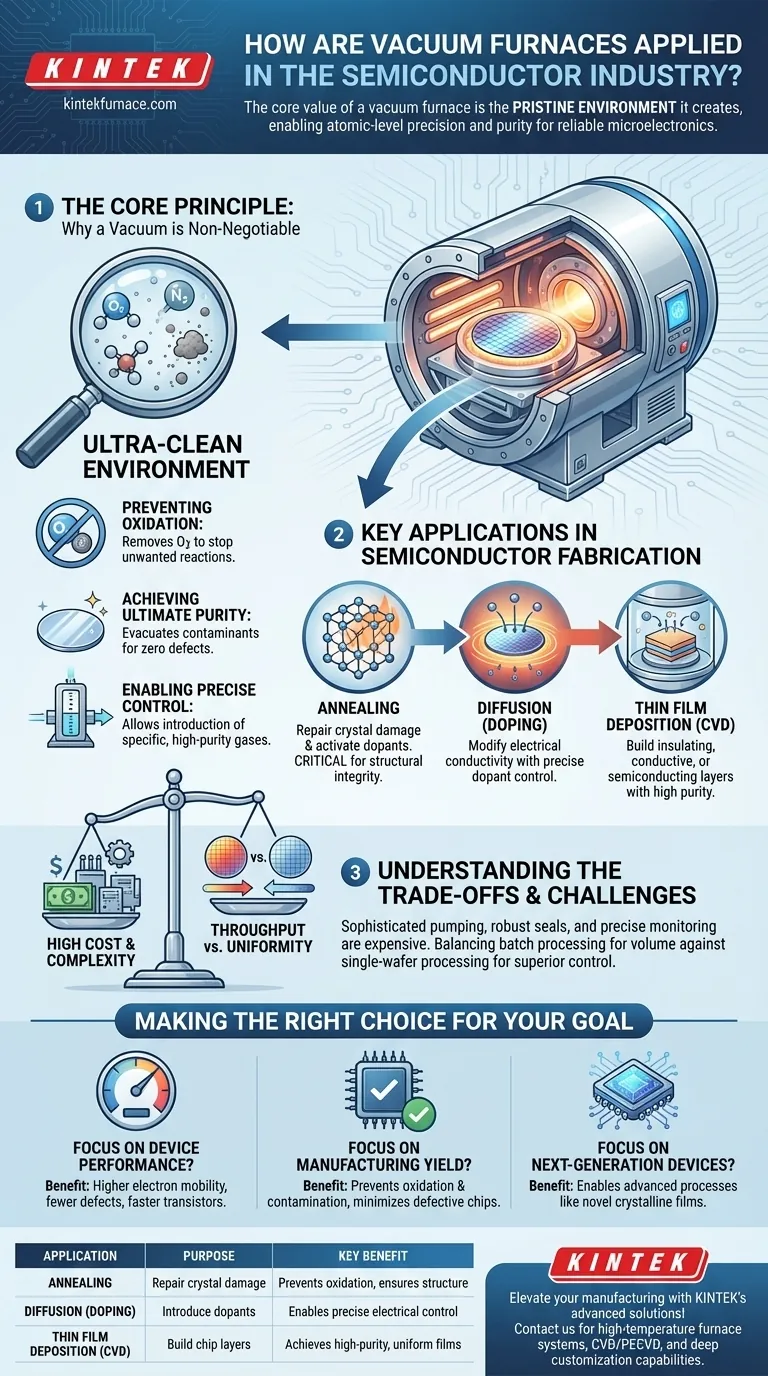
The core value of a vacuum furnace in semiconductor manufacturing is not just the heat it provides, but the pristine environment it creates. By removing virtually all atmospheric gases, it enables atomic-level precision and purity, which is the fundamental requirement for creating reliable, high-performance microelectronics.
The Core Principle: Why a Vacuum is Non-Negotiable
To understand the role of vacuum furnaces, you must first understand why the ambient air we breathe is the primary enemy of semiconductor fabrication. Air is filled with reactive gases and particles that are devastating at the nanometer scale.
Preventing Unwanted Chemical Reactions
The most significant threat is oxidation. Silicon, the foundation of virtually all semiconductors, reacts readily with oxygen at the high temperatures used in manufacturing. This forms an uncontrolled layer of silicon dioxide, altering the wafer's electrical properties and ruining the intended circuit design. A vacuum removes the oxygen, preventing this unwanted reaction.
Achieving Ultimate Purity
A modern microprocessor contains billions of transistors in a space smaller than a postage stamp. Even a single microscopic dust particle or a few stray atoms of an unwanted element can create a fatal defect. A vacuum furnace evacuates these contaminants, creating an environment of extreme purity that is impossible to achieve in open air.
Enabling Precise Control
Once a clean vacuum is established, engineers can introduce specific, high-purity gases in precisely controlled amounts. This is the basis for processes like doping and chemical vapor deposition, where the furnace becomes a sealed reaction chamber, ensuring that only the desired elements interact with the wafer surface.
Key Applications in Semiconductor Fabrication
While the principle is simple—remove the air—the applications are highly sophisticated. Vacuum furnaces are used at several critical stages of turning a raw silicon wafer into a finished chip.
Annealing: Repairing and Activating Wafers
Processes like ion implantation, which embed dopant atoms into the silicon, cause significant damage to the silicon's crystal structure. Annealing is a controlled heating process that repairs this damage. Performing it in a vacuum is critical to ensure the high temperature doesn't cause unintended oxidation while the crystal lattice reforms.
Diffusion (Doping): Modifying Electrical Properties
Doping is the process of intentionally introducing impurities (dopants) like boron or phosphorus into the silicon to change its electrical conductivity. In a diffusion furnace, a type of vacuum furnace, high temperatures cause these dopant atoms to spread, or "diffuse," into the wafer. The vacuum ensures the dopant concentration is precisely controlled and no other impurities are introduced.
Thin Film Deposition: Building the Chip's Layers
Modern chips are not monolithic; they are complex, three-dimensional structures built from dozens of layers. Chemical Vapor Deposition (CVD) is a process where gases react on the wafer's surface inside a furnace to deposit ultra-thin films. These films can be insulators (like silicon dioxide), conductors (like polysilicon), or semiconductors. A vacuum is essential for the purity and structural quality of these deposited layers.
Understanding the Trade-offs and Challenges
While essential, vacuum furnaces are not simple tools. They come with inherent complexities and limitations that engineers must manage.
High Cost and Complexity
Vacuum furnaces are expensive to build and operate. Achieving and maintaining a high vacuum requires sophisticated, energy-intensive pumping systems, robust seals, and advanced monitoring equipment. The complexity increases with the required temperature and level of vacuum.
Throughput vs. Uniformity
Traditional furnaces often processed wafers in large batches to maximize throughput. However, achieving perfect temperature and gas flow uniformity across every wafer in a large batch is challenging. This can lead to slight variations between chips. Many modern facilities have shifted to single-wafer processing for superior control, at the cost of lower throughput.
Process-Specific Designs
The term "vacuum furnace" describes a category, not a single device. A furnace designed for a low-temperature anneal is vastly different from a high-temperature CVD reactor. Each process requires a unique combination of temperature capabilities, gas delivery systems, and chamber materials, adding to the overall cost and complexity of a fabrication plant.
Making the Right Choice for Your Goal
The application of vacuum technology is directly tied to the final performance and reliability of the semiconductor device. Understanding this link clarifies its importance.
- If your primary focus is device performance: The ultimate purity achieved in a vacuum furnace directly translates to higher electron mobility and fewer defects, enabling faster and more power-efficient transistors.
- If your primary focus is manufacturing yield: Preventing oxidation and particle contamination through vacuum processing is the single most important factor in minimizing defective chips and maximizing the output of a fabrication facility.
- If your primary focus is creating next-generation devices: Advanced processes like growing novel crystalline films for optoelectronics or power devices are only possible in the ultra-controlled environment of a specialized vacuum furnace.
Ultimately, mastering the environment inside the furnace is the first step to mastering the behavior of electrons in the final product.
Summary Table:
| Application | Purpose | Key Benefit |
|---|---|---|
| Annealing | Repair crystal damage from ion implantation | Prevents oxidation, ensures structural integrity |
| Diffusion (Doping) | Introduce dopants to modify conductivity | Enables precise control of electrical properties |
| Thin Film Deposition (CVD) | Build insulating, conductive, or semiconducting layers | Achieves high-purity, uniform film quality |
Elevate your semiconductor manufacturing with KINTEK's advanced vacuum furnace solutions! Leveraging exceptional R&D and in-house manufacturing, we provide diverse laboratories with high-temperature furnace systems tailored for the semiconductor industry. Our product line—including Muffle, Tube, Rotary Furnaces, Vacuum & Atmosphere Furnaces, and CVD/PECVD Systems—is enhanced by strong deep customization capabilities to precisely meet your unique experimental needs. Achieve superior purity, precise control, and higher yields for processes like annealing, doping, and thin-film deposition. Contact us today to discuss how we can optimize your fabrication processes and drive innovation in your projects!
Visual Guide
Related Products
- Vacuum Hot Press Furnace Machine Heated Vacuum Press Tube Furnace
- Vacuum Hot Press Furnace Machine Heated Vacuum Press
- 600T Vacuum Induction Hot Press Vacuum Heat Treat and Sintering Furnace
- 2200 ℃ Tungsten Vacuum Heat Treat and Sintering Furnace
- Vacuum Heat Treat Sintering Furnace with Pressure for Vacuum Sintering
People Also Ask
- How does a vacuum hot press furnace promote densification in the manufacturing of graphite flake/copper composites? Achieve Superior Composite Materials
- What is the primary function of the vacuum environment in a vacuum hot press furnace during titanium alloy processing? Prevent Embrittlement for Superior Ductility
- Why is a high vacuum environment crucial when preparing copper-carbon nanotube composites in a vacuum hot press furnace? Achieve Superior Composite Integrity
- Why use Vacuum Hot Press (VHP) for ZnS Ceramics? Achieve Superior IR Transparency and Mechanical Strength
- What control features does a vacuum hot press furnace offer? Precision Control for Advanced Materials Processing


