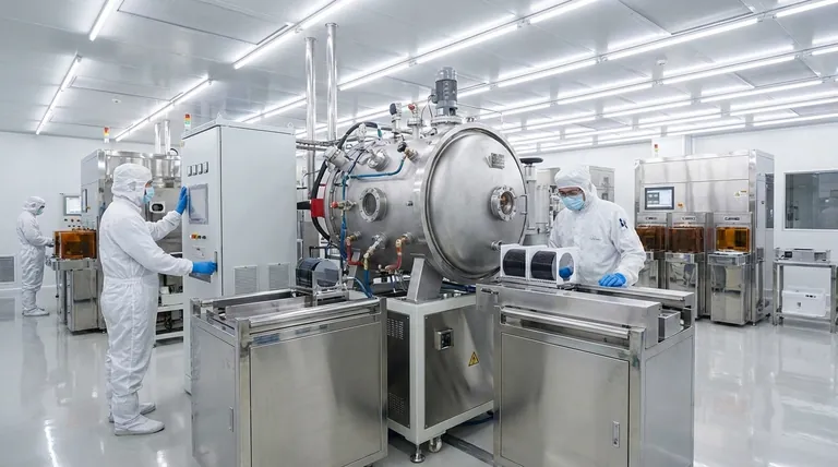
At the heart of every modern microchip lies a series of processes conducted in an environment of extreme purity. Vacuum furnaces are indispensable in semiconductor manufacturing for precision heat treatment, thin film deposition, and material modification. They create a controlled, contamination-free atmosphere that is essential for fabricating reliable and high-performance electronic components on silicon wafers.
The core challenge in semiconductor manufacturing is manipulating materials at a near-atomic scale without introducing defects. Vacuum furnaces solve this by removing atmospheric gases and particles, creating the pristine environment required for processes like annealing, deposition, and doping to succeed.
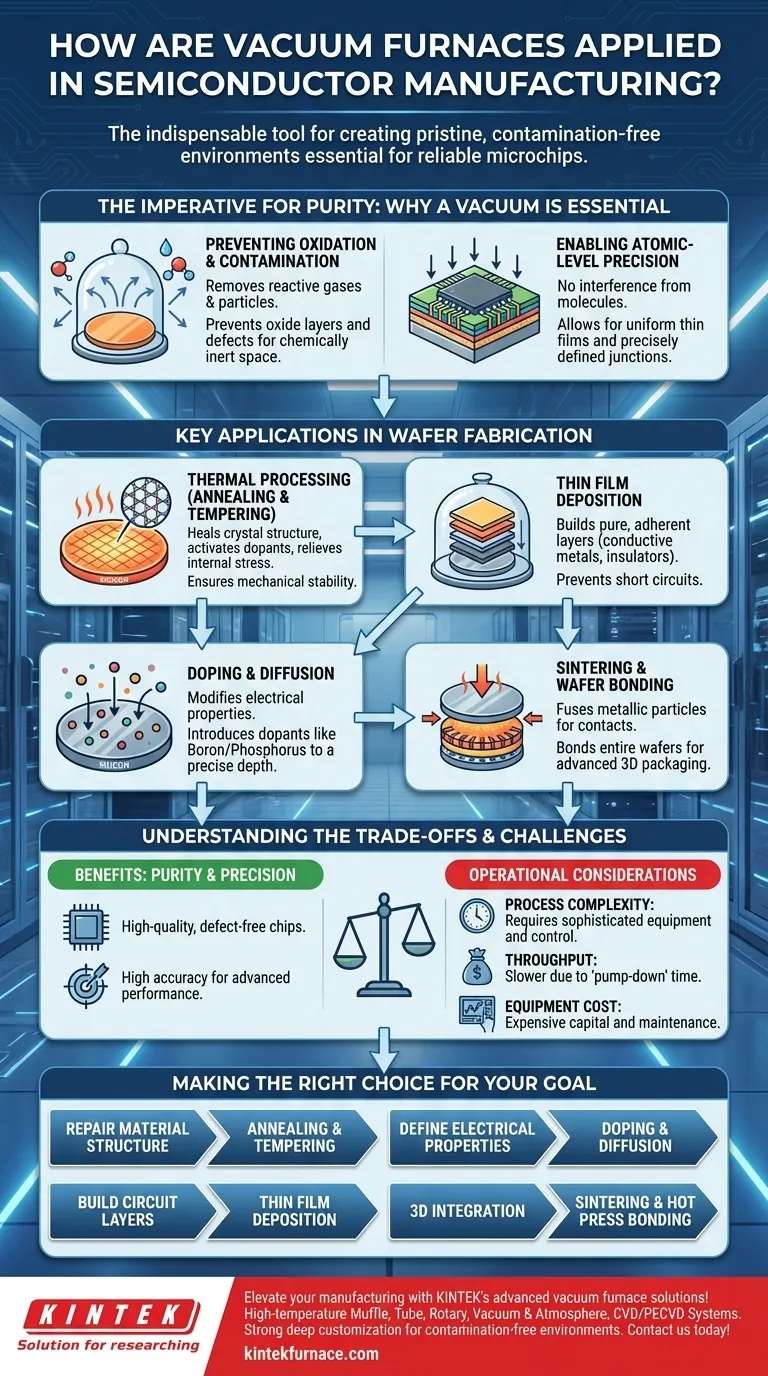
The Imperative for Purity: Why a Vacuum is Essential
The defining characteristic of a semiconductor is its precisely controlled impurity level. The manufacturing environment must therefore be cleaner and more controlled than almost any other industrial setting.
Preventing Oxidation and Contamination
In a normal atmosphere, oxygen and moisture react instantly with a heated silicon wafer, forming an uncontrolled oxide layer and introducing defects. Airborne dust and other microscopic particles can land on the wafer, ruining the microscopic circuits being built.
A vacuum removes these reactive gases and particles, creating a chemically inert space. This prevents unwanted reactions and ensures the only materials present are those intentionally introduced for the process.
Enabling Atomic-Level Precision
Processes like doping (introducing specific impurities) and thin film deposition (building circuit layers atom by atom) require absolute control.
In a vacuum, there are no other molecules to interfere with the path of a deposited atom or an implanted ion. This allows for the creation of perfectly uniform layers and precisely defined electrical junctions, which are the foundation of a functioning transistor.
Key Applications in Wafer Fabrication
Vacuum furnaces are used across the wafer fabrication lifecycle. While different furnace types exist, such as tubular furnaces for general processing and hot press furnaces for bonding, they all enable a core set of critical applications.
Thermal Processing: Annealing and Tempering
After processes like ion implantation damage the wafer's crystal structure, it must be repaired. Annealing is a high-temperature heating process that allows the silicon crystal lattice to heal, activating the implanted dopants.
Related processes like tempering and hardening are used to relieve internal stresses within the material layers, ensuring the final chip is mechanically stable and reliable.
Thin Film Deposition
Modern chips are built vertically with dozens of interconnected layers. Thin film deposition is the process of adding these layers, which can be conductive metals or insulating dielectrics.
Performing this in a vacuum ensures the deposited film is incredibly pure and adheres perfectly to the surface below, preventing short circuits or open circuits.
Doping and Diffusion
The electrical properties of silicon are modified by doping—the intentional introduction of elements like boron or phosphorus.
A vacuum furnace provides the high-temperature environment needed for these dopants to diffuse, or spread out, into the silicon crystal lattice to a precise depth and concentration.
Sintering and Wafer Bonding
Sintering is a heat treatment used to fuse metallic particles, often to form reliable electrical contacts on the chip.
For advanced 3D packaging, specialized hot press furnaces apply both heat and pressure in a vacuum to bond entire wafers together, creating complex, multi-layered devices.
Understanding the Trade-offs and Challenges
While essential, using vacuum furnaces is not without its complexities. The benefits of purity and precision come with operational considerations.
Process Complexity and Control
Achieving and maintaining a high vacuum requires sophisticated equipment and expert oversight. Process parameters like temperature ramps, pressure levels, and gas flow must be controlled with extreme accuracy, as any deviation can compromise the entire batch of wafers.
Throughput vs. Quality
Creating a high-vacuum environment takes time, a process known as "pump-down." This can make vacuum-based processes slower than their atmospheric counterparts. Manufacturers must constantly balance the need for high-quality, defect-free chips against the pressure for high-volume production.
Equipment Cost and Maintenance
High-vacuum furnaces and their associated pumps are specialized, expensive capital equipment. They demand rigorous and costly maintenance schedules to ensure they remain free of leaks and contamination, which could jeopardize production.
Making the Right Choice for Your Goal
The specific vacuum furnace process you utilize is dictated entirely by your manufacturing objective at that particular stage.
- If your primary focus is repairing material structure: You will rely on annealing and tempering to heal the crystal lattice and manage internal material stress.
- If your primary focus is building circuit layers: Your key process is thin film deposition, which requires the purest vacuum to create defect-free conductive and insulating layers.
- If your primary focus is defining electrical properties: You will use doping and diffusion to precisely introduce impurities and create the P-N junctions that form transistors.
- If your primary focus is 3D integration: You will leverage hot press furnaces to achieve high-precision wafer-to-wafer bonding under vacuum conditions.
Mastering these vacuum-based thermal processes is fundamental to fabricating the powerful and reliable semiconductor devices that underpin our modern world.
Summary Table:
| Application | Key Process | Purpose in Semiconductor Manufacturing |
|---|---|---|
| Thermal Processing | Annealing, Tempering | Heals crystal lattice, relieves stress, activates dopants |
| Thin Film Deposition | Deposition | Builds pure, adherent conductive/insulating layers |
| Doping and Diffusion | Doping, Diffusion | Modifies electrical properties with precise impurity control |
| Sintering and Bonding | Sintering, Wafer Bonding | Fuses particles for contacts, bonds wafers in 3D packaging |
Elevate your semiconductor manufacturing with KINTEK's advanced vacuum furnace solutions! Leveraging exceptional R&D and in-house manufacturing, we provide diverse laboratories with high-temperature furnaces like Muffle, Tube, Rotary, Vacuum & Atmosphere, and CVD/PECVD Systems. Our strong deep customization capability ensures precise alignment with your unique experimental needs, delivering contamination-free environments for superior chip performance. Contact us today to discuss how our tailored solutions can optimize your processes and drive innovation!
Visual Guide
Related Products
- Vacuum Hot Press Furnace Machine Heated Vacuum Press Tube Furnace
- Vacuum Hot Press Furnace Machine Heated Vacuum Press
- 600T Vacuum Induction Hot Press Vacuum Heat Treat and Sintering Furnace
- 2200 ℃ Tungsten Vacuum Heat Treat and Sintering Furnace
- Vacuum Heat Treat Sintering Furnace with Pressure for Vacuum Sintering
People Also Ask
- Why is a high vacuum environment crucial when preparing copper-carbon nanotube composites in a vacuum hot press furnace? Achieve Superior Composite Integrity
- How does the uniaxial pressure applied by a vacuum hot press furnace affect the microstructure of ZrC-SiC materials?
- How does a vacuum hot press furnace promote densification in the manufacturing of graphite flake/copper composites? Achieve Superior Composite Materials
- Which process parameters must be optimized for specific materials in a vacuum hot press furnace? Achieve Optimal Density and Microstructure
- What is the primary function of the vacuum environment in a vacuum hot press furnace during titanium alloy processing? Prevent Embrittlement for Superior Ductility


