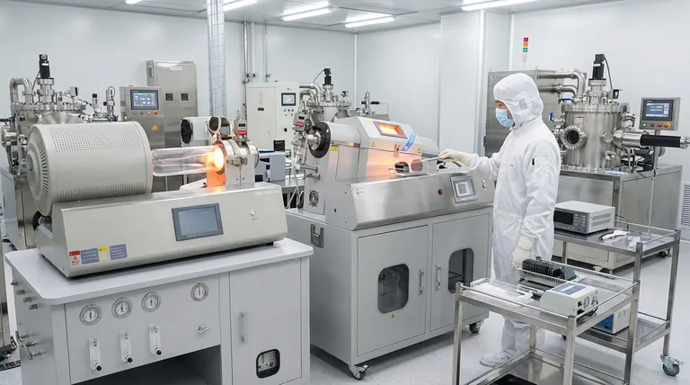
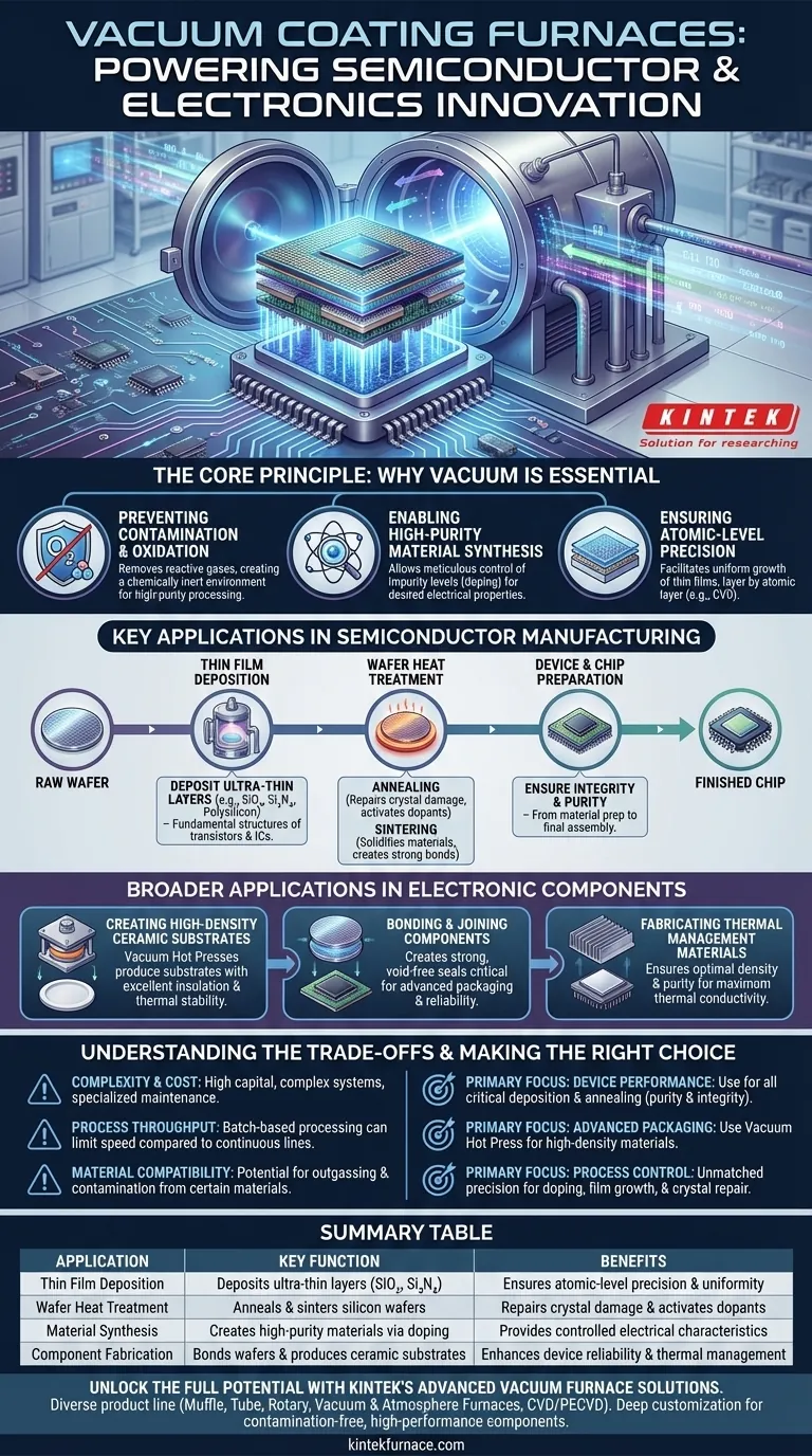
In the semiconductor and electronics industries, vacuum coating furnaces are indispensable tools used to deposit ultra-thin material layers, heat-treat silicon wafers, and synthesize high-purity materials for advanced components. These furnaces create a highly controlled, contamination-free environment that is the absolute prerequisite for fabricating reliable, high-performance microchips, circuits, and other sensitive electronic devices.
The core function of a vacuum furnace is not just to heat material, but to do so in an environment stripped of reactive gases. This prevents oxidation and contamination, enabling the atomic-level precision and material purity that modern electronics demand.
The Core Principle: Why Vacuum is Essential
The defining feature of a semiconductor is its precisely engineered impurity. Any uncontrolled variable, including a single stray atom of oxygen, can compromise the entire device. Vacuum furnaces are the primary defense against this.
Preventing Contamination and Oxidation
At the high temperatures required for manufacturing, materials like silicon are highly reactive. Exposing them to a normal atmosphere would cause immediate oxidation and contamination, destroying their delicate electronic properties.
A vacuum furnace removes virtually all atmospheric gases, creating a chemically inert environment. This ensures that the only reactions that occur are the ones intended by the process engineer.
Enabling High-Purity Material Synthesis
Vacuum furnaces are used to create materials with meticulously controlled impurity levels, a process known as doping. By operating in a near-perfect vacuum, engineers can introduce specific elements in precise quantities to give a semiconductor its desired electrical characteristics.
This level of control is impossible in any environment other than a high-vacuum chamber.
Ensuring Atomic-Level Precision
Modern microchips feature components that are only a few atoms thick. Vacuum deposition processes, such as Chemical Vapor Deposition (CVD), allow for the growth of these thin films with exceptional uniformity and precision, layer by atomic layer.
Key Applications in Semiconductor Manufacturing
From the raw wafer to the finished chip, vacuum furnaces are involved at nearly every critical stage of fabrication.
Thin Film Deposition
This is a cornerstone of chip manufacturing. Furnaces are used to deposit thin, uniform layers of materials that act as insulators, conductors, or semiconductors.
Commonly deposited films include silicon dioxide (SiO₂), silicon nitride (Si₃N₄), and polycrystalline silicon (polysilicon), which form the fundamental structures of transistors and integrated circuits.
Wafer Heat Treatment (Annealing & Sintering)
After processes like ion implantation (doping), the crystal structure of the silicon wafer is damaged. Annealing is a high-temperature heat treatment in a vacuum that repairs this damage and electrically activates the implanted dopants.
Sintering is another heat treatment process used to solidify materials or create strong bonds between different layers on the chip.
Device and Chip Preparation
The entire lifecycle of a chip involves multiple heat treatment steps within a vacuum. This ensures the integrity and purity of the device are maintained from its initial material preparation through to final assembly.
Broader Applications in Electronic Components
The use of vacuum furnaces extends beyond the silicon chip itself to the components that support it.
Creating High-Density Ceramic Substrates
Vacuum Hot Presses are specialized furnaces that apply both heat and pressure in a vacuum. They are used to produce the high-density ceramic substrates that microchips are mounted on, ensuring excellent electrical insulation and thermal stability.
Bonding and Joining Components
Vacuum furnaces are used to bond entire silicon wafers together or to join circuits to their substrates. This creates strong, void-free seals that are critical for advanced packaging techniques and device reliability.
Fabricating Thermal Management Materials
High-performance electronics generate significant heat. Vacuum furnaces help create advanced thermal management materials, such as heat spreaders and insulators, by ensuring optimal material density and purity for maximum thermal conductivity.
Understanding the Trade-offs
While essential, vacuum furnace technology is not without its challenges. Understanding these limitations is key to effective implementation.
Complexity and Cost
Vacuum furnaces are highly sophisticated and expensive pieces of equipment. They require significant capital investment, complex control systems, and specialized maintenance to manage the high-vacuum and high-temperature environments.
Process Throughput
Creating and maintaining a high vacuum is time-consuming. As a result, many vacuum processes are batch-based, which can limit throughput compared to continuous, atmospheric-pressure manufacturing lines.
Material Compatibility
Not all materials are suitable for vacuum processing. Some materials may outgas (release trapped volatiles) when exposed to a vacuum, which can contaminate the chamber and compromise the process.
Making the Right Choice for Your Process
The application of vacuum technology must be aligned with the specific manufacturing goal.
- If your primary focus is device performance: You must use vacuum furnaces for all critical deposition and annealing steps to guarantee the material purity and structural integrity required for high-speed, reliable chips.
- If your primary focus is advanced packaging or substrates: A Vacuum Hot Press is the correct tool for creating high-density ceramic or composite materials with superior thermal and electrical properties.
- If your primary focus is process control: The precision of vacuum environments is unmatched for doping, film growth, and repairing crystal damage, making it the only viable option for cutting-edge semiconductor nodes.
Ultimately, the vacuum furnace is the invisible workhorse that makes the entire modern electronics industry possible.
Summary Table:
| Application | Key Function | Benefits |
|---|---|---|
| Thin Film Deposition | Deposits ultra-thin layers (e.g., SiO₂, Si₃N₄) | Ensures atomic-level precision and uniformity |
| Wafer Heat Treatment | Anneals and sinters silicon wafers | Repairs crystal damage and activates dopants |
| Material Synthesis | Creates high-purity materials via doping | Provides controlled electrical characteristics |
| Component Fabrication | Bonds wafers and produces ceramic substrates | Enhances device reliability and thermal management |
Unlock the full potential of your semiconductor and electronic manufacturing with KINTEK's advanced vacuum furnace solutions. Leveraging exceptional R&D and in-house manufacturing, we offer a diverse product line including Muffle, Tube, Rotary, Vacuum & Atmosphere Furnaces, and CVD/PECVD Systems. Our strong deep customization capability ensures precise alignment with your unique experimental requirements, delivering contamination-free environments for high-performance components. Contact us today to discuss how we can enhance your process efficiency and product reliability!
Visual Guide
Related Products
- Vacuum Hot Press Furnace Machine for Lamination and Heating
- Small Vacuum Heat Treat and Tungsten Wire Sintering Furnace
- 2200 ℃ Graphite Vacuum Heat Treat Furnace
- Vacuum Heat Treat Furnace with Ceramic Fiber Liner
- Vacuum Sealed Continuous Working Rotary Tube Furnace Rotating Tube Furnace
People Also Ask
- What safety features are incorporated in vacuum hot press furnaces? Ensure Operator and Equipment Protection
- Why is a high vacuum environment crucial when preparing copper-carbon nanotube composites in a vacuum hot press furnace? Achieve Superior Composite Integrity
- What control features does a vacuum hot press furnace offer? Precision Control for Advanced Materials Processing
- What is the primary function of the vacuum environment in a vacuum hot press furnace during titanium alloy processing? Prevent Embrittlement for Superior Ductility
- What are the benefits of the vacuum environment system in a vacuum hot press furnace? Unlock High-Density Sintering


