The Frustration of "Almost Right" 2D Materials
You’ve prepared your silicon substrates, deposited your platinum-selenium (Pt-Se) composites, and followed the standard literature. Yet, when you take your samples to the Raman spectrometer or the SEM, the results are disappointing. Instead of the sharp, definitive peaks of high-quality crystalline Platinum Selenide (PtSe2), you see the broad, messy signals of an amorphous composite.
The material is there, but the property you need—the high carrier mobility or the specific bandgap—is missing. For researchers and semiconductor engineers, this is a common and costly roadblock. You are not just losing time; you are burning through expensive precursors and delaying critical project milestones.
The Common Struggle: Why "Close Enough" Temperatures Fail
When faced with poor crystallization, the typical reaction is to increase the heat or extend the time. However, many labs find that simply "cranking up the oven" leads to even worse outcomes:
- Oxidation: If the environment isn't perfectly inert, your platinum reacts with trace oxygen rather than selenium.
- Substrate Damage: Inconsistent thermal ramping can cause delamination from the silicon wafer.
- Incomplete Transformation: Without precise dwell times, the atoms simply don't have the "energy budget" to find their proper place in the crystal lattice.
The business consequence is clear: wasted laboratory resources, inconsistent data that can't be published or scaled, and a slower path to market for next-generation sensors or electronic components.
The Science of Atomic Rearrangement: Why 500°C and 5 Hours Matter
To understand the solution, we have to look at what is happening at the atomic level. An amorphous Pt-Se composite is like a box of disorganized building blocks. To transform it into a crystalline PtSe2 phase, you must facilitate a process called atomic rearrangement.
This isn't a simple heating task; it is a delicate thermodynamic dance.
- The Thermal Threshold: Research indicates that 500 °C is the critical "sweet spot." It provides enough kinetic energy for the platinum and selenium atoms to break their temporary, disordered bonds and migrate into a stable, hexagonal lattice.
- The Element of Time: This migration isn't instantaneous. It requires a sustained dwell time—typically 5 hours—to ensure the transformation is uniform across the entire substrate.
- The Shield of Argon: Because selenium is volatile and platinum is sensitive at high temperatures, this process must occur under a strict Argon atmosphere. Any fluctuation in gas purity or pressure during those five hours can ruin the phase purity of the film.
Standard furnaces often suffer from "thermal overshoot" or "cold spots," meaning part of your sample might reach 510°C while another stays at 480°C. In the world of 2D materials, that 30-degree difference is the gap between a breakthrough and a failure.
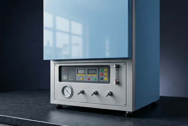
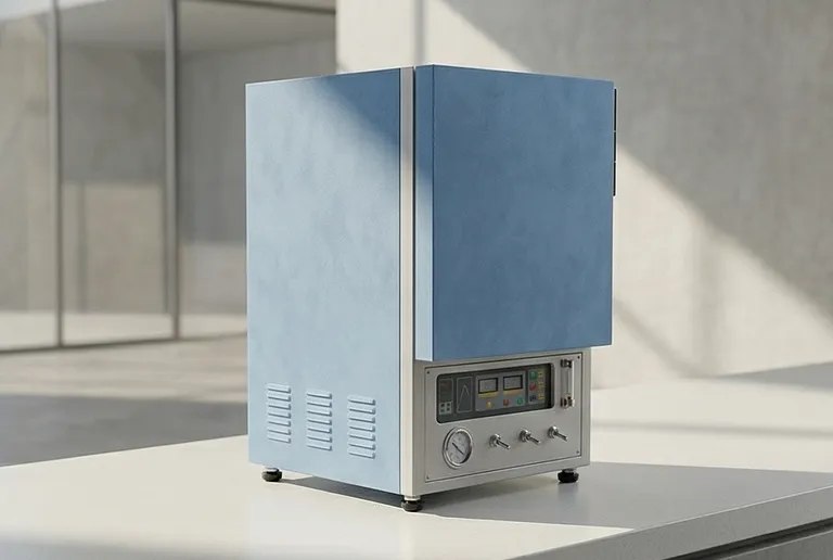
The Solution: A CVD System Designed for Phase Precision
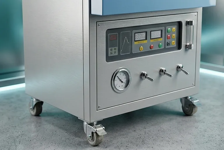
True crystalline transformation requires more than just heat; it requires a controlled environment where every variable is locked down. This is where a specialized Chemical Vapor Deposition (CVD) system becomes an essential tool rather than a luxury.
A high-performance CVD system, such as those engineered by KINTEK, acts as a precision reactor. It addresses the root causes of synthesis failure through:
- Ultra-Stable Thermal Control: Maintaining a rock-steady 500°C for the full 5-hour duration, ensuring uniform crystallization across every square millimeter of the substrate.
- Atmospheric Integrity: Integrated mass flow controllers and high-vacuum seals ensure the Argon environment remains pure, preventing the oxidation that plagues lesser systems.
- Process Repeatability: By automating the ramp, dwell, and cool-down cycles, the system removes "human error," allowing you to produce the same high-quality PtSe2 phase every single time.
Our CVD equipment isn't just a furnace; it is a catalyst for the transition from "amorphous composite" to "functional crystalline material."
Beyond the Fix: Unlocking the Potential of PtSe2
When the hurdle of synthesis is cleared, the real work begins. By reliably producing high-quality crystalline PtSe2, you move beyond troubleshooting and into innovation.
Stable, crystalline PtSe2 opens the door to:
- High-Performance Photodetectors: Utilizing the material's thickness-dependent bandgap.
- Next-Gen Spintronics: Leveraging the strong spin-orbit coupling of high-purity crystals.
- Scalable Semiconductor Manufacturing: Transitioning from small-scale lab experiments to reproducible, wafer-scale production.
Don't let inconsistent hardware hold back your material science breakthroughs. Whether you are struggling with phase transformation or looking to scale your CVD process, our team is ready to help you optimize your thermal environment.
Ready to achieve crystalline perfection in your 2D material synthesis? Contact our expert consultants today to discuss your specific temperature and atmosphere requirements and find the ideal furnace configuration for your research goals. [Contact Our Experts](#ContactForm)
Related Products
- Controlled Inert Nitrogen Hydrogen Atmosphere Furnace
- Custom Made Versatile CVD Tube Furnace Chemical Vapor Deposition CVD Equipment Machine
- Split Chamber CVD Tube Furnace with Vacuum Station CVD Machine
- Multi Heating Zones CVD Tube Furnace Machine for Chemical Vapor Deposition Equipment
- Slide PECVD Tube Furnace with Liquid Gasifier PECVD Machine
Related Articles
- Why Your Silicon Carbide Ceramics Are Brittle: The Invisible Role of Argon Atmosphere
- Why Your Galfenol Sheets Fail to Recrystallize—And How Precise Atmosphere Control Unlocks High Performance
- The Hidden Flaw in Your Heat Treatment: It’s Not the Temperature, It’s the Air
- Why Your High-Temperature Materials Fail: The Hidden Enemy in Your Furnace
- Beyond Temperature: Why Your Material Processing Fails and How to Fix It


