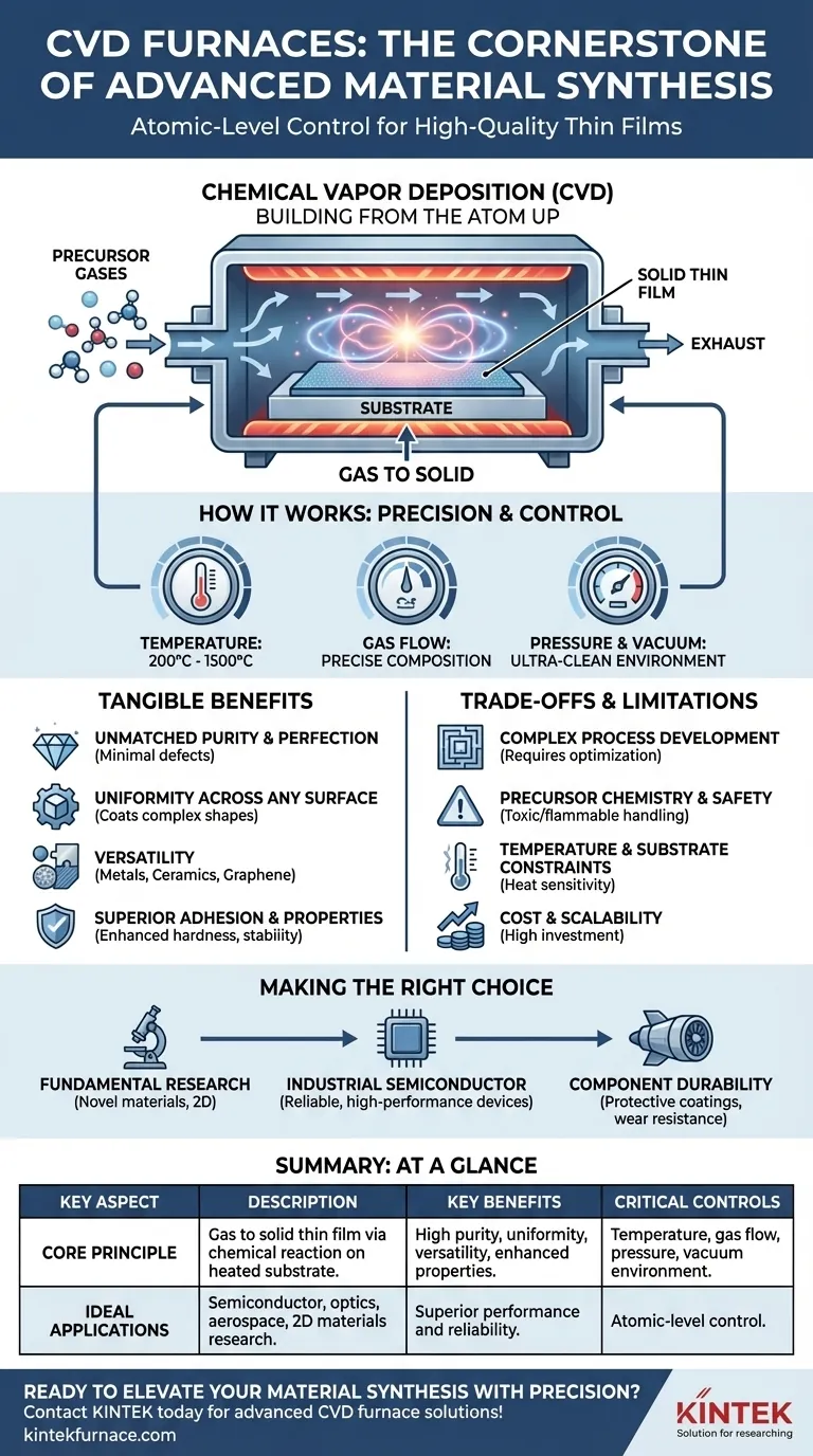
At its core, a Chemical Vapor Deposition (CVD) furnace is a cornerstone of advanced material synthesis because it provides an unparalleled level of control for building high-quality, uniform thin films from the atom up. By precisely managing a chemical reaction in an ultra-clean environment, it enables the creation of materials with specific, enhanced properties that are indispensable for industries ranging from semiconductor manufacturing to optics and aerospace.
The true value of a CVD furnace lies not just in its ability to generate heat, but in its function as a micro-fabrication chamber. It offers the precise control over temperature, pressure, and gas chemistry required to transform gaseous precursors into solid, high-purity materials with tailored atomic structures.
How a CVD Furnace Fundamentally Works
To understand its importance, you must first understand its process. A CVD furnace is not merely an oven; it is a sophisticated chemical reactor.
From Gas to Solid: The Core Principle
The process begins by introducing specific precursor gases into the furnace chamber. These gases flow over a heated object, known as a substrate. The high temperature triggers a chemical reaction, causing the gases to decompose and deposit a solid thin film onto the substrate's surface.
The Critical Role of the Controlled Environment
CVD furnaces operate under a vacuum or a tightly controlled atmosphere. This pristine, contamination-free environment is essential for eliminating impurities and preventing unwanted side reactions. This control is what guarantees the high purity of the final material.
Precision Through Control Systems
The furnace allows for meticulous management of several key parameters:
- Temperature: Often ranging from 200°C to over 1500°C, temperature dictates the rate and nature of the chemical reaction.
- Gas Flow: Precise control over the flow rate of each precursor gas determines the composition of the final film.
- Pressure: The chamber pressure (from vacuum to atmospheric) influences gas behavior and deposition uniformity.
By adjusting these levers, an operator can fine-tune the resulting film's thickness, composition, and crystalline structure with remarkable accuracy.
The Tangible Benefits of CVD Synthesis
This precise control translates directly into superior material outcomes that are difficult or impossible to achieve with other methods.
Unmatched Purity and Perfection
Because the deposition occurs in a controlled vacuum environment, the resulting films have minimal defects and a highly controlled composition. This is a non-negotiable requirement for applications like semiconductors, where a single atomic impurity can ruin a device.
Uniformity Across Any Surface
Unlike line-of-sight deposition methods, the gaseous nature of the CVD process allows it to coat complex, three-dimensional shapes with a perfectly uniform layer. This ensures consistent performance across the entire surface of a component.
Versatility in Material Creation
CVD is an incredibly flexible platform. It is not limited to one type of material and is routinely used to deposit a wide range of substances, including metals, advanced ceramics, polymers, and even revolutionary 2D materials like graphene.
Superior Adhesion and Enhanced Properties
The deposition process forms strong chemical bonds between the film and the substrate, resulting in excellent adhesion. The films themselves can be engineered to dramatically improve a material's hardness, thermal stability, corrosion resistance, or optical characteristics.
Understanding the Trade-offs and Limitations
While powerful, the CVD process is not without its challenges. Objectivity requires acknowledging its complexities.
The Complexity of Process Development
Developing a new CVD process is a significant undertaking. Achieving the desired film properties requires extensive experimentation to optimize the intricate balance between temperature, pressure, and gas chemistry for a specific material and substrate.
Precursor Chemistry and Safety
The precursor gases used in CVD can be highly toxic, flammable, or corrosive. This necessitates robust safety protocols, specialized handling equipment, and efficient exhaust management systems, adding to the operational complexity and cost.
Temperature and Substrate Constraints
The high temperatures required for many CVD processes limit the types of substrates that can be used. Materials with low melting points or those that are sensitive to thermal stress may not be compatible.
Cost and Scalability
While scalable from lab research to industrial production, the initial capital investment for a CVD system can be substantial. The ongoing costs of precursor gases, vacuum pumps, and energy consumption are also key considerations.
Making the Right Choice for Your Goal
The decision to use a CVD furnace should be driven by the specific demands of your application.
- If your primary focus is fundamental research (e.g., 2D materials): The furnace's atomic-level control over thickness and purity is essential for synthesizing novel materials.
- If your primary focus is industrial semiconductor fabrication: The unmatched uniformity and purity of CVD films at scale are critical for producing reliable, high-performance electronic devices.
- If your primary focus is enhancing component durability (e.g., protective coatings): The superior adhesion and tailored properties like hardness and corrosion resistance justify the investment in CVD technology.
Ultimately, leveraging a CVD furnace is about designing and constructing materials with a level of precision that begins at the atomic scale.
Summary Table:
| Key Aspect | Description |
|---|---|
| Core Principle | Transforms gaseous precursors into solid thin films via controlled chemical reactions on a heated substrate. |
| Key Benefits | High purity, uniform coating on complex shapes, versatility in materials (e.g., graphene, ceramics), and enhanced properties like adhesion and durability. |
| Critical Controls | Temperature (200°C to 1500°C), gas flow, pressure, and vacuum environment for contamination-free synthesis. |
| Ideal Applications | Semiconductor manufacturing, optics, aerospace, and research in 2D materials for superior performance and reliability. |
| Limitations | High complexity in process development, safety concerns with toxic precursors, substrate temperature constraints, and significant cost and scalability considerations. |
Ready to elevate your material synthesis with precision and reliability? At KINTEK, we leverage exceptional R&D and in-house manufacturing to provide advanced high-temperature furnace solutions tailored to your needs. Our product line includes CVD/PECVD Systems, Muffle, Tube, Rotary Furnaces, and Vacuum & Atmosphere Furnaces, all backed by strong deep customization capabilities to meet your unique experimental requirements. Whether you're in semiconductor fabrication, aerospace, or materials research, we help you achieve atomic-level control and superior outcomes. Contact us today to discuss how our CVD furnaces can drive your innovations forward!
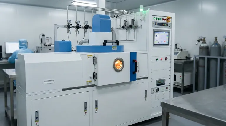
Visual Guide
Related Products
- Custom Made Versatile CVD Tube Furnace Chemical Vapor Deposition CVD Equipment Machine
- Split Chamber CVD Tube Furnace with Vacuum Station CVD Machine
- Multi Heating Zones CVD Tube Furnace Machine for Chemical Vapor Deposition Equipment
- Slide PECVD Tube Furnace with Liquid Gasifier PECVD Machine
- Controlled Inert Nitrogen Hydrogen Atmosphere Furnace
People Also Ask
- How can integrating CVD tube furnaces with other technologies benefit device fabrication? Unlock Advanced Hybrid Processes
- What is a CVD tube furnace and what is its primary function? Discover Precision Thin-Film Deposition
- How does CVD tube furnace sintering enhance graphene growth? Achieve Superior Crystallinity and High Electron Mobility
- What are the benefits of developing new precursor materials for CVD tube furnaces? Unlock Advanced Thin-Film Synthesis
- What are the practical applications of gate media prepared by CVD tube furnaces? Unlock Advanced Electronics and More


