Surface passivation is critical for CVD coatings because it creates a chemically clean, stable, and uniform foundation on the substrate. This preparation is essential for ensuring the deposited film adheres strongly, grows without defects, and possesses the desired chemical and physical properties. Without it, the coating is likely to fail.
The quality of a Chemical Vapor Deposition (CVD) coating is dictated by the quality of the substrate surface it is grown upon. Surface passivation is not an optional step; it is the fundamental process of preparing that substrate to ensure the success of the coating.
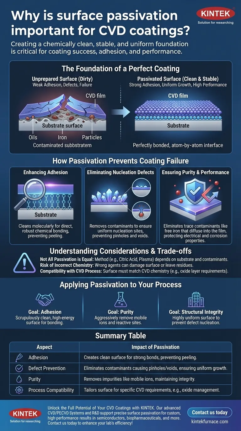
The Foundation of a Perfect Coating
To understand the importance of passivation, we must first recognize that a CVD coating is not merely painted on. It is grown atom-by-atom from a chemical reaction at the substrate's surface.
What is a CVD Coating?
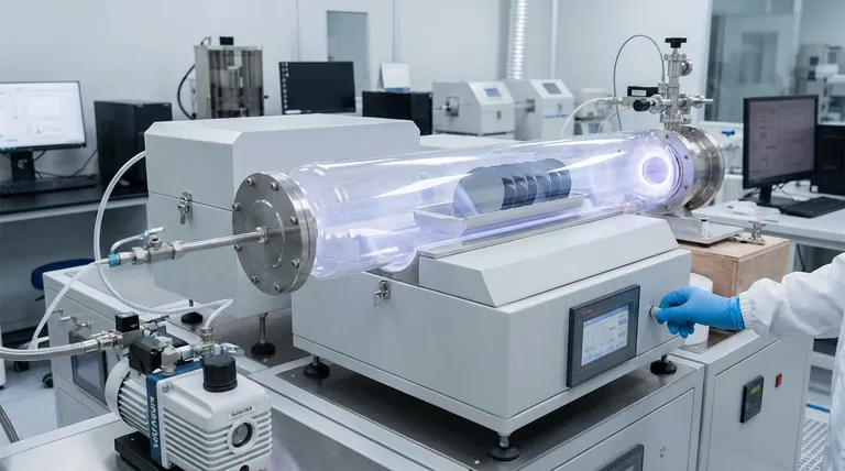
Chemical Vapor Deposition (CVD) is a process where a substrate is exposed to one or more volatile chemical precursors, which react and/or decompose on the substrate surface to produce the desired thin film.
The success of this atomic-level assembly depends entirely on the condition of the very first layer of atoms it encounters—the substrate surface.
Defining Passivation for CVD
While often associated with removing free iron from stainless steel to prevent rust, passivation in the context of high-technology coatings has a broader meaning. It is any process that makes a surface "passive" or non-reactive in a controlled way.
This involves removing unwanted contaminants (like oils, particles, and mobile ions like free iron) and creating a chemically stable, uniform surface layer. This prepared surface acts as the ideal template for the CVD film to grow upon.
How Passivation Prevents Coating Failure
An unprepared substrate is the most common cause of CVD coating failure. Passivation directly addresses the primary failure modes.
Enhancing Adhesion
A CVD film needs strong chemical bonds to the substrate to adhere properly. Surface contaminants create a weak boundary layer, preventing these bonds from forming and leading to peeling or flaking of the coating.
Passivation cleans the surface at a molecular level, exposing the underlying substrate material so the coating can form a direct, robust bond.
Eliminating Nucleation Defects
The CVD film begins to grow at specific "nucleation sites." On an ideal surface, these sites are uniform, leading to a smooth, dense film.
Contaminants or defects on the surface, such as microscopic particles or areas of free iron, act as unwanted nucleation points. This results in a non-uniform film with pinholes, voids, or other structural defects that compromise its integrity.
Ensuring Purity and Performance
In high-purity applications like semiconductors or biopharmaceuticals, even trace contaminants on the substrate can be devastating. These impurities can diffuse from the surface into the growing film during the high-temperature CVD process.
This contamination can alter the coating's electrical properties, reduce its corrosion resistance, or create reactive sites on a surface that must be inert. Passivation removes these sources of contamination before the coating process begins.
Understanding the Trade-offs and Considerations
Passivation is a crucial step, but it must be executed correctly. The wrong approach can be more damaging than doing nothing at all.
Not All Passivation is Created Equal
The specific passivation method—whether it's a citric acid treatment, a different chemical etch, or a plasma clean—must be carefully selected.
The choice depends on the substrate material (e.g., stainless steel, silicon, titanium), the type of contaminants to be removed, and the specific requirements of the subsequent CVD process.
The Risk of Incorrect Chemistry
Using the wrong chemical agent, concentration, or temperature can damage the substrate. Over-etching can roughen the surface in an uncontrolled way, creating new defects.
An incorrect process might also leave behind chemical residues that are just as detrimental as the original contaminants, defeating the purpose of the step entirely.
Compatibility with the CVD Process
The final passivated surface must be compatible with the CVD chemistry. Some processes require a specific, thin, stable oxide layer to initiate growth, which is itself a form of passivation. Other processes might require the complete removal of all oxides. This coordination is critical.
Applying Passivation to Your Process
The specific passivation strategy should be directly tied to the primary goal of your coating.
- If your primary focus is maximizing adhesion: The goal is to create a scrupulously clean, high-energy surface free of organic and metallic contaminants to promote strong chemical bonding.
- If your primary focus is ensuring chemical purity: The passivation must aggressively remove mobile ions and reactive sites, such as the free iron that causes rouging in stainless steel systems.
- If your primary focus is the coating's structural integrity: The passivation must create a highly uniform surface to prevent defect nucleation points that compromise the final film's density and uniformity.
Ultimately, treating the preparation of the substrate with as much rigor as the coating process itself is the only path to achieving consistent, high-performance results.
Summary Table:
| Aspect | Impact of Passivation |
|---|---|
| Adhesion | Creates a clean surface for strong chemical bonds, preventing peeling or flaking. |
| Defect Prevention | Eliminates contaminants that cause pinholes and voids, ensuring uniform film growth. |
| Purity | Removes impurities like mobile ions, maintaining coating integrity in sensitive applications. |
| Process Compatibility | Tailors the surface for specific CVD requirements, such as oxide layer management. |
Unlock the Full Potential of Your CVD Coatings with KINTEK
Struggling with coating failures or inconsistent results? Our advanced high-temperature furnace solutions, including CVD/PECVD Systems, are engineered to support precise surface passivation and deposition processes. Leveraging exceptional R&D and in-house manufacturing, KINTEK offers deep customization to meet your unique experimental needs—ensuring strong adhesion, defect-free films, and high purity for applications in semiconductors, biopharmaceuticals, and more.
Contact us today to discuss how our tailored solutions can enhance your lab's efficiency and coating performance!
Visual Guide
Related Products
- HFCVD Machine System Equipment for Drawing Die Nano Diamond Coating
- RF PECVD System Radio Frequency Plasma Enhanced Chemical Vapor Deposition
- Custom Made Versatile CVD Tube Furnace Chemical Vapor Deposition CVD Equipment Machine
- Multi Heating Zones CVD Tube Furnace Machine for Chemical Vapor Deposition Equipment
People Also Ask
- What core function does CVD equipment serve in h-BN anti-corrosion? Master Precision Synthesis for High-Performance Films
- What is the function of high-purity Argon (Ar) gas during CVD? Optimize Your Thin Film Uniformity and Purity
- What are the equipment for chemical vapor deposition? A Guide to the 5 Essential Components
- What is the advantage of using a CVD system for coating turbine blades? Master Complex Geometries with Ease
- What is chemical vapor deposition (CVD) and its primary industrial application? Unlock Precision Thin Films for Electronics


