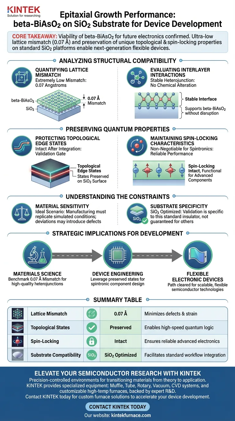
The investigation of epitaxial growth performance of beta-BiAsO2 on a SiO2 substrate is a prerequisite for transitioning this material from theoretical physics to practical device application. This specific study is necessary to quantify the lattice mismatch—which is remarkably low at 0.07 Angstroms—and to verify that the material's interlayer interactions with the substrate do not disrupt its intrinsic electronic behaviors.
Core Takeaway: The viability of beta-BiAsO2 for future electronics depends entirely on how well it interfaces with standard substrates. This analysis confirms that despite the physical bonding process, the material retains the unique topological and spin-locking properties required for next-generation flexible devices.
Analyzing Structural Compatibility
To successfully integrate a new material into semiconductor workflows, the physical connection between layers must be nearly perfect.
Quantifying Lattice Mismatch
The primary metric for growth success is the lattice mismatch.
In the case of beta-BiAsO2 on SiO2, simulations reveal a mismatch of only 0.07 Angstroms. This extremely low number suggests that the crystalline structures align closely, minimizing the strain that typically leads to defects.
Evaluating Interlayer Interactions
Beyond simple geometry, the chemical and physical interactions between layers define the heterojunction's stability.
Studying the epitaxial growth allows researchers to model these interactions precisely. This ensures that the SiO2 substrate supports the beta-BiAsO2 layer without chemically altering it or introducing instability that would degrade performance over time.
Preserving Quantum Properties
Structural stability is useless if the material loses the electronic characteristics that make it valuable.
Protecting Topological Edge States
Beta-BiAsO2 is prized for its unique topological edge states.
The growth study serves as a validation gate to ensure these states are not destroyed by the substrate's influence. The findings confirm that these delicate quantum states remain intact even after the material is integrated onto the SiO2 surface.
Maintaining Spin-Locking Characteristics
For spintronic applications, the "spin-locking" capability of the material is non-negotiable.
The epitaxial analysis confirms that the heterojunction model preserves these characteristics. This proves that the material can function as intended in advanced electronic components, rather than acting merely as an inert layer.
Understanding the Constraints
While the results are promising, it is vital to recognize the specific boundaries of this confirmation.
Material Sensitivity
The preservation of properties is highly dependent on achieving the simulated lattice conditions.
Even though the mismatch is only 0.07 Angstroms, deviations during actual physical fabrication could introduce defects. The study highlights an ideal scenario that manufacturing processes must strive to replicate.
Substrate Specificity
The validation is specific to the SiO2 interface.
While SiO2 is a standard insulator in electronics, success here does not automatically guarantee similar performance on other substrate types without conducting similar epitaxial studies.
Strategic Implications for Development
The results of this study provide a roadmap for utilizing beta-BiAsO2 in tangible applications, specifically pointing toward flexible electronic devices.
- If your primary focus is Materials Science: Prioritize the 0.07 Angstrom mismatch data as a benchmark for high-quality heterojunction formation.
- If your primary focus is Device Engineering: Leverage the confirmation of preserved topological states to design spintronic components using standard SiO2 platforms.
By validating that beta-BiAsO2 can survive integration without losing its quantum identity, this study clears the path for its adoption in scalable, flexible semiconductor technologies.
Summary Table:
| Key Metric | Value / Status | Impact on Device Performance |
|---|---|---|
| Lattice Mismatch | 0.07 Å | Minimizes crystalline defects and structural strain |
| Topological States | Preserved | Enables high-speed quantum and spintronic logic |
| Spin-Locking | Intact | Ensures reliable performance in advanced electronics |
| Substrate Compatibility | SiO2 Optimized | Facilitates integration with standard semiconductor workflows |
Elevate Your Semiconductor Research with KINTEK
Transitioning materials like beta-BiAsO2 from theory to application requires precision-controlled environments. KINTEK provides the specialized equipment needed for advanced materials science. Backed by expert R&D and manufacturing, we offer Muffle, Tube, Rotary, Vacuum, and CVD systems, alongside other laboratory high-temp furnaces—all fully customizable to your unique research needs.
Ready to achieve near-perfect epitaxial growth and preserve critical quantum properties in your lab? Contact KINTEK today to discuss your custom furnace solution and see how our expertise can accelerate your device development.
Visual Guide
References
- Exploring a new topological insulator in β-BiAs oxide. DOI: 10.1039/d5ra01911g
This article is also based on technical information from Kintek Furnace Knowledge Base .