Graphene nanoribbons are considered candidates for digital devices because they solve a fundamental flaw of pure graphene: they possess an electronic bandgap. While bulk graphene is an excellent conductor, it cannot be effectively "switched off," making it unsuitable for transistors. By shaping graphene into ultra-narrow ribbons, a bandgap is created, enabling the on/off switching action that is the basis of all digital logic.
The core issue with pure graphene for digital electronics is its lack of a bandgap, preventing it from acting as a switch. Creating nanoribbons induces this necessary bandgap through a principle called quantum confinement, but the extreme precision required during manufacturing remains a significant barrier to practical application.
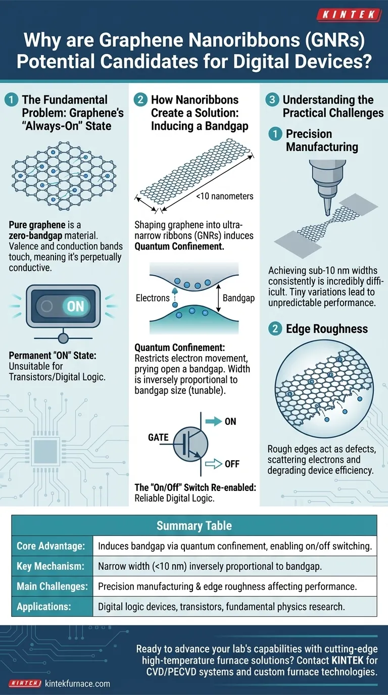
The Fundamental Problem: Graphene's "Always-On" State
To understand the promise of nanoribbons, we must first understand the limitation of their parent material, graphene. The challenge lies in a property called the electronic bandgap.
What Is a Bandgap?
A bandgap is the minimum energy required to excite an electron from a non-conducting state (the valence band) to a conducting state (the conduction band).
Materials like silicon have a bandgap, which allows us to control the flow of electricity. By applying a voltage, we can give electrons enough energy to jump this gap and turn the current "on." Removing the voltage leaves the electrons without enough energy, turning the current "off."
Graphene's Missing Bandgap
Pure graphene is a "zero-bandgap" material. Its valence and conduction bands touch, meaning it takes virtually no energy to make electrons flow.
This makes graphene perpetually conductive. A transistor built from it would be permanently "on," which is useless for a digital switch that must represent both 1s (on) and 0s (off).
How Nanoribbons Create a Solution
Graphene nanoribbons (GNRs) overcome this limitation by fundamentally changing the material's electronic structure through its physical dimensions.
Introducing Quantum Confinement
When graphene is shaped into an extremely narrow ribbon—typically less than 10 nanometers wide—the electrons are spatially restricted. This effect is known as quantum confinement.
Think of electrons flowing in a wide sheet of graphene like water in a vast ocean. In a nanoribbon, they are forced into a narrow channel. This confinement restricts their movement and changes their allowed energy levels, effectively prying open a bandgap where one did not exist before.
The Critical Role of Width
The size of this induced bandgap is inversely proportional to the ribbon's width. The narrower the GNR, the larger the bandgap becomes.
This tunability is powerful. It suggests we could engineer GNRs with specific bandgaps tailored for different applications, much like we do with different semiconductor materials today.
The "On/Off" Switch Re-enabled
With a bandgap in place, a GNR-based transistor can finally function as a proper switch. Applying a gate voltage can push electrons across the gap to turn the device ON, and removing it allows the device to turn fully OFF, enabling reliable digital logic.
Understanding the Practical Challenges
While the theory is promising, the path to using GNRs in commercial devices is defined by significant manufacturing hurdles.
The Challenge of Precision Manufacturing
Achieving the required sub-10 nm widths consistently and at scale is incredibly difficult. Even tiny variations in the width of a single ribbon can alter its electronic properties, leading to unpredictable device performance.
The Problem of "Edge Roughness"
The edges of the nanoribbon must be perfectly smooth at an atomic level. Any rough or irregular edges act as defects that scatter electrons as they travel down the ribbon.
This scattering disrupts the smooth flow of current, degrading the device's performance and efficiency, much like friction slows down an object in motion.
Making the Right Choice for Your Goal
Evaluating the potential of graphene nanoribbons requires understanding their current position on the spectrum from fundamental research to applied technology.
- If your primary focus is fundamental physics research: GNRs are an excellent platform for studying the effects of quantum confinement and exploring novel electronic phenomena.
- If your primary focus is near-term commercial application: The immense challenges in fabrication precision and edge control mean GNRs remain a long-term prospect, not a drop-in replacement for silicon.
Understanding both the quantum principles that give GNRs their potential and the fabrication hurdles that currently limit them is key to charting their future in digital electronics.
Summary Table:
| Aspect | Details |
|---|---|
| Core Advantage | Induces a bandgap via quantum confinement, enabling on/off switching for transistors |
| Key Mechanism | Narrow width (<10 nm) inversely proportional to bandgap size |
| Main Challenges | Precision manufacturing and edge roughness affecting performance |
| Applications | Digital logic devices, transistors, and fundamental physics research |
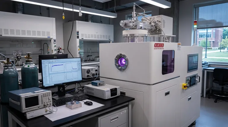
Ready to advance your lab's capabilities with cutting-edge high-temperature furnace solutions? At KINTEK, we leverage exceptional R&D and in-house manufacturing to provide diverse laboratories with advanced solutions like Muffle, Tube, Rotary Furnaces, Vacuum & Atmosphere Furnaces, and CVD/PECVD Systems. Our strong deep customization capability ensures we precisely meet your unique experimental requirements, helping you overcome challenges in materials research and development. Contact us today to discuss how our tailored furnace technologies can drive your innovations forward!
Visual Guide
Related Products
- Multi Heating Zones CVD Tube Furnace Machine for Chemical Vapor Deposition Equipment
- Small Vacuum Heat Treat and Tungsten Wire Sintering Furnace
- HFCVD Machine System Equipment for Drawing Die Nano Diamond Coating
- 2200 ℃ Graphite Vacuum Heat Treat Furnace
- 1200℃ Controlled Inert Nitrogen Atmosphere Furnace
People Also Ask
- What is the function of a multi-zone tube furnace in CVD synthesis? Master 2D In2Se3 Nanosheet Precision
- What role do multi zone tube furnaces play in new energy research? Unlock Precise Thermal Control for Innovation
- What are the benefits of integrating multiple heating zones in a tube furnace? Unlock Precise Thermal Control
- What role does a Tube Furnace play in the CVD growth of carbon nanotubes? Achieve High-Purity CNT Synthesis
- Why are multi zone tube furnaces particularly useful for nanomaterial research? Unlock Precise Thermal Control for Advanced Synthesis