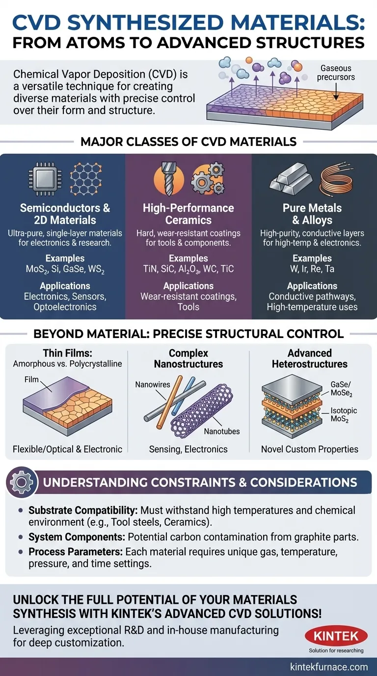
At its core, Chemical Vapor Deposition (CVD) is an exceptionally versatile technique capable of synthesizing a vast range of materials. These materials span multiple categories, including advanced two-dimensional (2D) materials like MoS2 and GaSe, high-performance ceramics such as titanium nitride, pure metals like tungsten and iridium, and fundamental semiconductors like silicon. The process can create everything from simple coatings to complex heterostructures.
The true power of CVD lies not just in the wide variety of materials it can produce, but in its precise control over their final form and structure—from amorphous thin films to crystalline nanowires and layered heterostructures.
The Major Classes of CVD Materials
CVD is not limited to a single industry or application. Its ability to deposit different material classes makes it a foundational technology in fields ranging from microelectronics to heavy industry.
Semiconductors and 2D Materials
CVD is the cornerstone of modern semiconductor fabrication and advanced materials research. It enables the creation of ultra-pure, single-layer materials with exceptional electronic and optical properties.
Specific examples include monolayers or few-layers of:
- Molybdenum disulfide (MoS2)
- Molybdenum diselenide (MoSe2)
- Tungsten disulfide (WS2)
- Gallium selenide (GaSe)
- Palladium diselenide (PdSe2)
- Elemental silicon
High-Performance Ceramics
CVD is widely used to deposit hard, wear-resistant, and chemically inert ceramic coatings onto tools and components, dramatically extending their lifespan.
These include nonoxide ceramics like carbides and nitrides, and oxide ceramics:
- Carbides: Tungsten carbide (WC), silicon carbide (SiC), tantalum carbide (TaC), titanium carbide (TiC)
- Nitrides: Titanium nitride (TiN), titanium carbonitride (TiCN)
- Oxides: Aluminum oxide (Al2O3), hafnia (HfO2), zirconia (ZrO2)
Pure Metals and Alloys
The technique can also deposit high-purity metallic layers, which are critical for creating conductive pathways in electronics or for applications requiring high-temperature and corrosion resistance.
Metals deposited via CVD include rhenium, tantalum, tungsten, and iridium. It can also be adapted to produce specific alloys.
Beyond Material Type: Controlling Structure and Form
Understanding CVD means looking beyond a simple list of materials. Its real advantage is the architectural control it provides at the micro and nano-scale.
Thin Films: Amorphous vs. Polycrystalline
CVD can dictate the atomic structure of the deposited film. It can create amorphous materials, which lack a crystalline structure and are valuable for flexible or optical devices.
It can also produce polycrystalline materials, which consist of many small crystalline grains. These are fundamental to products like solar panels and many electronic components.
Complex Nanostructures
The process is not limited to flat films. With precise control over conditions, CVD can be used to grow intricate structures like nanowires and nanotubes, which have unique properties and applications in sensing, electronics, and composites.
Advanced Heterostructures
For cutting-edge research and devices, CVD can layer different materials on top of one another (vertical heterostructures) or grow them side-by-side (lateral heterostructures).
Examples like GaSe/MoSe2 or isotopic MoS2 heterostructures allow engineers to design materials with entirely new, custom-tailored electronic or photonic properties that do not exist in a single material.
Understanding the Trade-offs and Constraints
While powerful, CVD is not without its operational constraints. The choice of material and substrate are deeply interconnected.
The Importance of Substrate Compatibility
The material being coated, known as the substrate, must be able to withstand the high temperatures and chemical environment of the CVD process.
Commonly used substrates include tungsten carbides, tool steels, high-temperature nickel alloys, ceramics, and graphite. The coating and substrate must be chemically and thermally compatible to ensure strong adhesion.
The Role of System Components
The CVD reactor itself can impose limitations. For example, many high-temperature systems use graphite hot zones and carbon-based insulation. This environment may be unsuitable for processes that are sensitive to carbon contamination.
Not a One-Size-Fits-All Process
A system set up to deposit tungsten carbide on tool steel cannot simply be used to grow monolayer graphene. Each material requires a unique combination of precursor gases, temperatures, pressures, and process times, often necessitating specialized equipment and expert process development.
Making the Right Choice for Your Application
Your specific goal will determine which facet of CVD's capability is most relevant.
- If your primary focus is next-generation electronics or research: CVD offers unparalleled precision for creating high-purity 2D materials, nanowires, and novel heterostructures.
- If your primary focus is protective coatings for tools or industrial components: The technology excels at depositing extremely hard and durable ceramic layers like TiN, TiC, and Al2O3.
- If your primary focus is specialized optical or flexible devices: CVD provides critical control over film structure, enabling the creation of amorphous or polycrystalline films with tailored properties.
Ultimately, Chemical Vapor Deposition is a foundational and adaptable platform for engineering materials from the atom up.
Summary Table:
| Material Class | Examples | Key Applications |
|---|---|---|
| Semiconductors & 2D Materials | MoS2, Si, GaSe | Electronics, sensors, optoelectronics |
| High-Performance Ceramics | TiN, SiC, Al2O3 | Wear-resistant coatings, tools |
| Pure Metals & Alloys | W, Ir, Re | Conductive pathways, high-temperature uses |
| Nanostructures & Heterostructures | Nanowires, GaSe/MoSe2 | Advanced devices, composites |
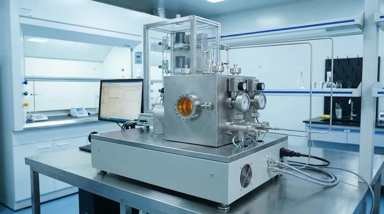
Unlock the full potential of your materials synthesis with KINTEK's advanced CVD solutions! Leveraging exceptional R&D and in-house manufacturing, we provide diverse laboratories with high-temperature furnace systems, including CVD/PECVD Systems, Muffle, Tube, Rotary, Vacuum & Atmosphere Furnaces. Our strong deep customization capability ensures precise alignment with your unique experimental needs—whether you're developing next-generation electronics, durable coatings, or complex heterostructures. Contact us today to discuss how our tailored solutions can enhance your research and production efficiency!
Visual Guide
Related Products
- HFCVD Machine System Equipment for Drawing Die Nano Diamond Coating
- Cylindrical Resonator MPCVD Machine System for Lab Diamond Growth
- Custom Made Versatile CVD Tube Furnace Chemical Vapor Deposition CVD Equipment Machine
- 915MHz MPCVD Diamond Machine Microwave Plasma Chemical Vapor Deposition System Reactor
- RF PECVD System Radio Frequency Plasma Enhanced Chemical Vapor Deposition
People Also Ask
- What is the function of high-purity Argon (Ar) gas during CVD? Optimize Your Thin Film Uniformity and Purity
- What is Hot-filament Chemical Vapor Deposition (HFCVD)? Achieve High-Quality Thin Films with Precision Control
- What is the significance of the vacuum pressure control system in the CVD coating process for powders?
- What core function does CVD equipment serve in h-BN anti-corrosion? Master Precision Synthesis for High-Performance Films
- What are the equipment for chemical vapor deposition? A Guide to the 5 Essential Components