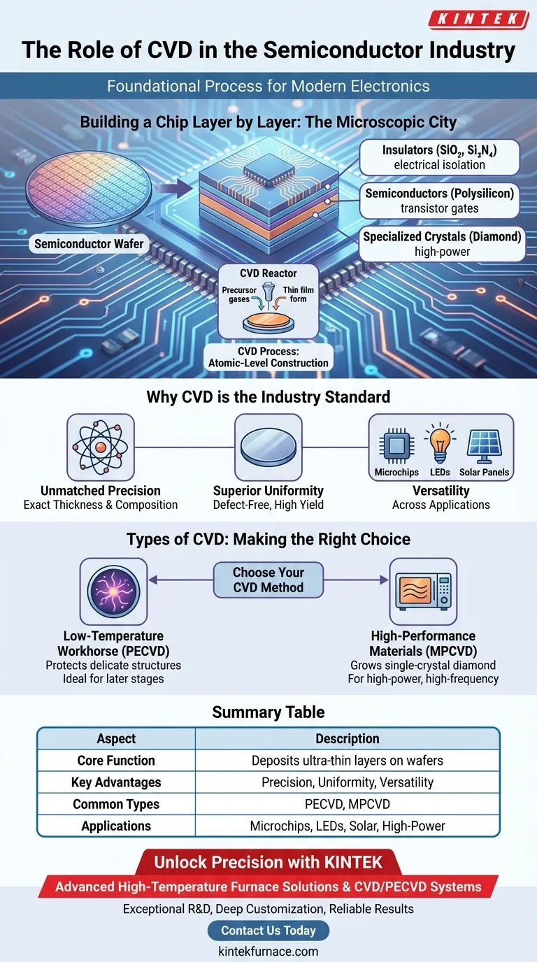
In the semiconductor industry, Chemical Vapor Deposition (CVD) is the foundational process for building the microscopic structures of modern electronics. It is a highly controlled method used to deposit ultra-thin layers of material onto a semiconductor wafer. These films create the essential insulating, conductive, and semiconducting components that form a complete integrated circuit (IC), making it indispensable for manufacturing everything from microprocessors to LEDs and solar cells.
At its core, semiconductor fabrication is an act of atomic-level construction. CVD is the primary tool for this construction, enabling engineers to build complex, multi-layered microchips by precisely depositing the exact materials needed for a device to function reliably and efficiently.
The Core Function: Building a Chip Layer by Layer
A modern microchip is not a single, flat object but a dense, three-dimensional city of electronic components. CVD is the technique used to build the floors, walls, and wiring of this microscopic city.
What is a Thin Film?
A thin film is a layer of material ranging from a few nanometers to several micrometers in thickness. In a chip, these films have distinct jobs: insulating one component from another, conducting electrical signals, or acting as the semiconductor material in a transistor.
The CVD Process in a Nutshell
The process involves introducing one or more volatile precursor gases into a reaction chamber, often called a furnace. These gases react and decompose on the surface of the semiconductor wafer, leaving behind a solid, high-purity thin film.
Essential Materials Deposited by CVD
CVD's versatility allows it to deposit all the fundamental material types required for an IC.
- Insulators (Dielectrics): Materials like silicon dioxide (SiO₂) and silicon nitride (Si₃N₄) are deposited to electrically isolate different conductive pathways, preventing short circuits.
- Semiconductors: Polysilicon is a critical semiconductor material deposited by CVD that forms the "gate" of a transistor, the switch that controls the flow of electricity.
- Specialized Crystals: Advanced CVD processes can even grow single-crystal diamond films, used for high-power electronics that require exceptional thermal management.
Why CVD is the Industry Standard
While other deposition methods exist, CVD remains dominant in semiconductor manufacturing due to a few non-negotiable advantages that are critical for producing advanced electronics.
Unmatched Precision and Control
CVD allows for precise, atomic-level control over the thickness and composition of the deposited film. As transistors shrink to the nanometer scale, this level of precision is not a luxury—it is a requirement.
Superior Uniformity and Quality
The process creates films that are exceptionally uniform and free of defects across the entire surface of a wafer. This ensures that every chip on the wafer performs identically and reliably, which is critical for achieving high manufacturing yields.
Versatility Across Applications
Beyond standard microchips, CVD is the go-to process for producing materials for LEDs and high-efficiency solar panels. The core principle of depositing high-quality, functional thin films applies across these different technologies.
Understanding the Trade-offs: Different Types of CVD
The term "CVD" is an umbrella for several specialized techniques. The choice of method depends on the material being deposited and the temperature sensitivity of the device being built.
PECVD: The Low-Temperature Workhorse
Plasma-Enhanced CVD (PECVD) uses a plasma to energize the precursor gases, allowing deposition to occur at much lower temperatures. This is vital in later manufacturing stages when a chip already has delicate structures that would be damaged by high heat. PECVD offers excellent control over film properties like mechanical stress and ensures minimal impurities.
MPCVD: For High-Performance Materials
Microwave-Plasma CVD (MPCVD) is a specialized technique used to grow high-purity, single-crystal diamond. Diamond's exceptional thermal conductivity and electrical properties enable the creation of high-frequency and high-power devices for defense, telecommunications, and high-performance computing.
Making the Right Choice for Your Goal
The selection of a specific CVD technique is driven by material requirements, thermal budget, and its precise role in the fabrication sequence.
- If your primary focus is standard insulation and transistor gates: Standard thermal CVD or PECVD for depositing SiO₂, Si₃N₄, and polysilicon is the industry's backbone.
- If your primary focus is protecting temperature-sensitive layers: PECVD is the essential choice due to its lower processing temperatures, which prevent damage to previously fabricated structures.
- If your primary focus is developing next-generation high-power or high-frequency electronics: A specialized technique like MPCVD is required to grow advanced materials like diamond that offer superior thermal and electrical performance.
Ultimately, mastering the various forms of CVD is synonymous with mastering the art of modern semiconductor manufacturing.
Summary Table:
| Aspect | Description |
|---|---|
| Core Function | Deposits ultra-thin layers (insulators, semiconductors) on wafers for integrated circuits |
| Key Advantages | High precision, uniformity, versatility for LEDs, solar cells, and microprocessors |
| Common CVD Types | PECVD (low-temperature), MPCVD (high-performance materials like diamond) |
| Applications | Microchips, LEDs, solar panels, high-power electronics |
Unlock Precision in Your Semiconductor Processes with KINTEK
Leveraging exceptional R&D and in-house manufacturing, KINTEK provides diverse laboratories with advanced high-temperature furnace solutions. Our product line, including Muffle, Tube, Rotary Furnaces, Vacuum & Atmosphere Furnaces, and CVD/PECVD Systems, is complemented by our strong deep customization capability to precisely meet unique experimental requirements. Whether you're developing next-generation electronics or optimizing production, our expertise ensures reliable, high-quality results tailored to your needs.
Contact us today to discuss how our CVD systems can enhance your semiconductor fabrication and drive innovation in your projects!
Visual Guide
Related Products
- Custom Made Versatile CVD Tube Furnace Chemical Vapor Deposition CVD Equipment Machine
- Split Chamber CVD Tube Furnace with Vacuum Station CVD Machine
- Multi Heating Zones CVD Tube Furnace Machine for Chemical Vapor Deposition Equipment
- Slide PECVD Tube Furnace with Liquid Gasifier PECVD Machine
- Controlled Inert Nitrogen Hydrogen Atmosphere Furnace
People Also Ask
- What are the key features of CVD tube furnaces for 2D material processing? Unlock Precision Synthesis for Superior Materials
- What temperature range do standard CVD tube furnaces operate at? Unlock Precision for Your Material Deposition
- What is a CVD tube furnace and what is its primary function? Discover Precision Thin-Film Deposition
- What improvements can be made to the bonding force of gate dielectric films using a CVD tube furnace? Enhance Adhesion for Reliable Devices
- Why are CVD tube furnace sintering systems indispensable for 2D material research and production? Unlock Atomic-Scale Precision


