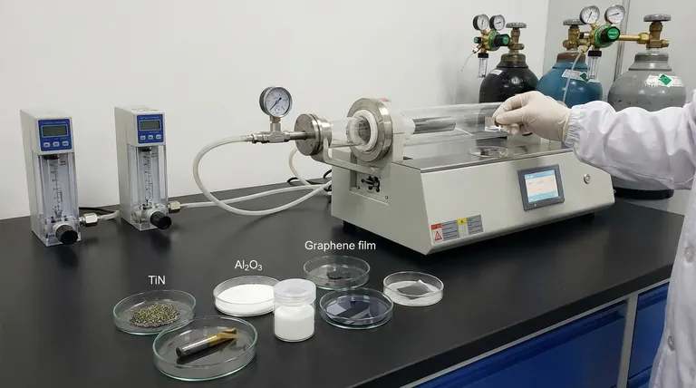
In Chemical Vapor Deposition (CVD), the most common materials used for coating are categorized into several key families. These include hard industrial materials like titanium nitride (TiN), titanium carbide (TiC), and aluminum oxide (Al2O3), foundational electronic materials like silicon compounds, specialized functional films like fluorocarbons, and cutting-edge 2D materials such as graphene and molybdenum disulfide (MoS2).
The materials used in CVD are not just a list of chemicals; they are a toolkit for engineering surfaces at the atomic level. The selection of a material is a strategic choice driven entirely by the final performance requirement, whether it's for wear resistance, electrical conductivity, or optical clarity.
A Functional Guide to CVD Material Families
Understanding CVD materials requires looking past the chemical names and focusing on the function they provide to the underlying part or substrate. Each family of materials delivers a distinct set of properties.
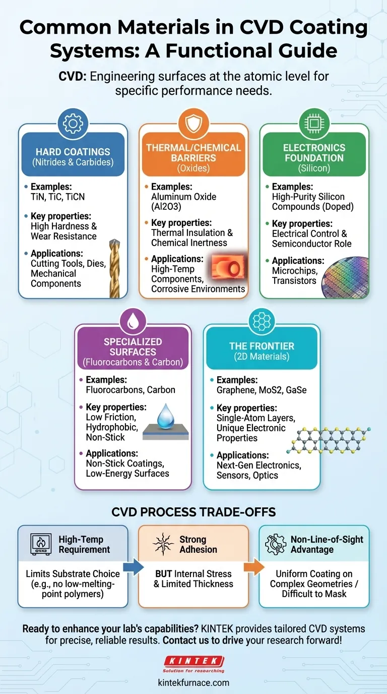
Hard Coatings: Nitrides and Carbides
Nitrides and carbides are the workhorses of industrial coatings, prized for their exceptional hardness and wear resistance.
Materials like titanium nitride (TiN), titanium carbide (TiC), and titanium carbonitride (TiCN) are deposited on cutting tools, dies, and mechanical components to dramatically extend their operational life.
Thermal and Chemical Barriers: Oxides
Oxides are chosen for their stability, creating a barrier that protects a substrate from high temperatures and corrosive chemical environments.
Aluminum oxide (Al2O3), often deposited in its alpha or kappa crystalline phase, is a prime example. It provides excellent thermal insulation and chemical inertness, making it vital for components used in high-temperature processes.
The Foundation of Electronics: Silicon
Silicon-based materials are the cornerstone of the semiconductor industry. CVD is a fundamental process for building the intricate layers that make up modern microchips.
The process allows for the deposition of high-purity silicon compounds. Critically, these layers can be doped during the CVD process to precisely control their electrical properties, functionalizing the surface for its role in a transistor or other electronic component.
Specialized Surfaces: Carbon and Fluorocarbons
This category includes materials designed for unique surface properties, such as low friction or chemical repellency.
Carbon films can be deposited in various forms, while fluorocarbons (or organofluorines) create surfaces with very low energy, similar to Teflon. These are used for non-stick, low-friction, or hydrophobic applications.
The Frontier: 2D Materials
CVD is at the forefront of nanomaterial synthesis, enabling the creation of single-atom-thick layers with extraordinary properties.
Materials like molybdenum disulfide (MoS2), gallium selenide (GaSe), and tungsten disulfide (WS2) are being developed for next-generation electronics, sensors, and optics. CVD can even create complex vertical or lateral "heterostructures" by stacking different 2D materials.
Understanding the Trade-offs of the CVD Process
While powerful, the CVD process has inherent characteristics that influence material selection and application. It is not a universal solution, and its trade-offs must be understood.
The High-Temperature Requirement
Most CVD reactions require elevated temperatures to proceed. This is a significant constraint, as it limits the types of substrates that can be coated. Materials with low melting points, like many polymers or certain aluminum alloys, cannot be used.
Adhesion vs. Stress
CVD creates a chemical bond between the coating and the substrate, resulting in superior adhesion compared to many other methods.
However, this process can also introduce internal stress into the film. As the coating gets thicker, this stress accumulates and can cause cracking or delamination, which limits the practical thickness of most CVD coatings.
The Non-Line-of-Sight Advantage
Unlike line-of-sight processes like PVD (Physical Vapor Deposition), the precursor gases in a CVD chamber can flow around and into complex geometries. This allows for a uniform coating on all exposed surfaces, which is a major advantage for intricate parts.
The downside is that this makes it difficult to mask or selectively coat only specific areas of a component.
Making the Right Choice for Your Goal
Your choice of a CVD material should be a direct reflection of your primary engineering objective.
- If your primary focus is mechanical wear resistance: Nitrides and carbides like TiN and TiC are the industry standard for hardening tools and components.
- If your primary focus is high-temperature or chemical protection: Aluminum Oxide (Al2O3) is the ideal choice for creating a stable, inert barrier.
- If your primary focus is semiconductor fabrication: Silicon-based materials are the cornerstone, allowing for precise doping to achieve specific electronic properties.
- If your primary focus is a unique surface property: Fluorocarbons for low-friction or hydrophobic surfaces are the most effective solution.
Ultimately, selecting the right CVD material is about defining your engineering goal first and then choosing the chemistry that achieves it.
Summary Table:
| Material Family | Common Examples | Key Properties | Typical Applications |
|---|---|---|---|
| Hard Coatings | TiN, TiC, TiCN | High hardness, wear resistance | Cutting tools, dies |
| Thermal/Chemical Barriers | Al2O3 | Thermal insulation, chemical inertness | High-temperature components |
| Electronics | Silicon compounds | High purity, electrical control | Semiconductors, microchips |
| Specialized Surfaces | Fluorocarbons | Low friction, hydrophobic | Non-stick coatings |
| 2D Materials | Graphene, MoS2 | Thin layers, unique electronic properties | Sensors, next-gen electronics |
Ready to enhance your lab's capabilities with advanced CVD solutions? At KINTEK, we leverage exceptional R&D and in-house manufacturing to provide high-temperature furnace systems tailored to your needs. Our product line includes Muffle, Tube, Rotary Furnaces, Vacuum & Atmosphere Furnaces, and CVD/PECVD Systems, all supported by deep customization to meet unique experimental requirements. Whether you're working with hard coatings, electronic materials, or cutting-edge 2D films, we can help you achieve precise, reliable results. Contact us today to discuss how our solutions can drive your research forward!
Visual Guide
Related Products
- HFCVD Machine System Equipment for Drawing Die Nano Diamond Coating
- RF PECVD System Radio Frequency Plasma Enhanced Chemical Vapor Deposition
- Cylindrical Resonator MPCVD Machine System for Lab Diamond Growth
- 915MHz MPCVD Diamond Machine Microwave Plasma Chemical Vapor Deposition System Reactor
- Custom Made Versatile CVD Tube Furnace Chemical Vapor Deposition CVD Equipment Machine
People Also Ask
- How can customers maximize the quality of CVD coatings? Master Pre-Coating Prep for Superior Results
- What role does Chemical Vapor Deposition (CVD) equipment play in the surface coating of carbon fibers for composites?
- What is the function of high-purity Argon (Ar) gas during CVD? Optimize Your Thin Film Uniformity and Purity
- What is the significance of the vacuum pressure control system in the CVD coating process for powders?
- What is the advantage of using a CVD system for coating turbine blades? Master Complex Geometries with Ease


