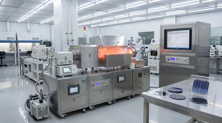
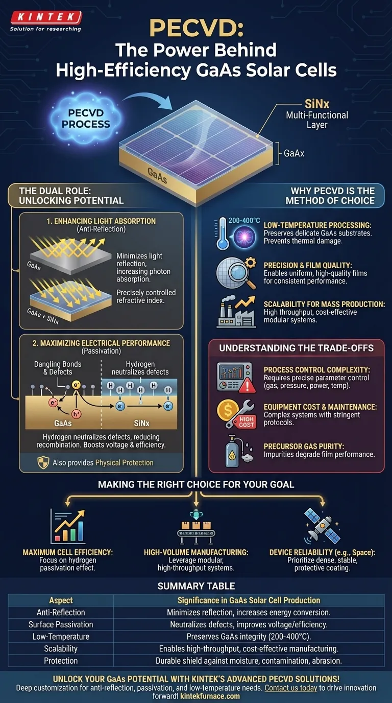
In the production of high-efficiency Gallium Arsenide (GaAs) solar cells, Plasma-Enhanced Chemical Vapor Deposition (PECVD) is not merely a step, but a critical enabling technology. Its primary significance lies in its ability to deposit thin films, such as silicon nitride (SiNx), that perform the dual functions of anti-reflection and surface passivation. This process directly enhances the cell's light absorption and electrical performance, making it indispensable for achieving the record-breaking efficiencies that define GaAs photovoltaics.
The core value of PECVD in this context is its low-temperature nature. This allows for the deposition of high-quality, performance-critical films onto delicate GaAs substrates without causing thermal damage, a limitation that prevents the use of many higher-temperature deposition methods.
The Dual Role of the PECVD Layer
The thin film deposited by PECVD is not just a simple coating; it is a multi-functional layer engineered to extract the maximum possible power from the solar cell. Its significance comes from two primary contributions.
Enhancing Light Absorption (Anti-Reflection)
A bare semiconductor surface like GaAs is naturally reflective, meaning a significant percentage of incoming sunlight bounces off before it can be converted into electricity.
PECVD is used to deposit a precisely controlled thin film of silicon nitride (SiNx). This layer is engineered with a specific refractive index that minimizes light reflection across the solar spectrum, ensuring more photons enter the active region of the cell.
Maximizing Electrical Performance (Passivation)
The surface of any crystal, including GaAs, contains imperfections like "dangling bonds" and dislocations. These defects act as traps for charge carriers (electrons and holes), causing them to recombine and be lost before they can contribute to the electrical current.
The PECVD process for depositing SiNx is often performed in a hydrogen-rich environment. This hydrogen gets incorporated into the film and diffuses to the GaAs surface, where it "passivates" or neutralizes these defects. This significantly reduces recombination losses, improves charge carrier mobility, and provides a direct boost to the cell's voltage and overall efficiency.
Providing Physical Protection
Beyond its optical and electrical roles, the hard, dense SiNx layer serves a practical purpose. It acts as a durable shield, protecting the sensitive underlying GaAs layers from moisture, contamination, and physical abrasion during handling and operation, which is especially critical for long-duration space missions.
Why PECVD is the Method of Choice
While other deposition methods exist, PECVD offers a unique combination of advantages that make it perfectly suited for high-performance GaAs solar cell manufacturing.
Low-Temperature Processing
This is the single most important advantage. Traditional Chemical Vapor Deposition (CVD) often requires very high temperatures that can degrade the sensitive crystal structure of the GaAs device.
PECVD uses an energy source—plasma—to activate the precursor gases. This allows the chemical reactions to occur at much lower substrate temperatures (typically 200-400°C), preserving the integrity and performance of the underlying cell structure.
Precision and Film Quality
The plasma process enables exceptionally uniform films with precise control over thickness, composition, and density. This consistency is essential for manufacturing large-area solar cells where every part of the cell must perform at the same high level.
Scalability for Mass Production
Modern PECVD systems are designed for high throughput and industrial-scale manufacturing. Features like modular designs, high uptime, and efficient use of raw materials make the process cost-effective for large-volume production, which is crucial for both terrestrial and space applications.
Understanding the Trade-offs
While indispensable, PECVD is a sophisticated process with its own set of operational considerations that must be managed for optimal results.
Process Control Complexity
The quality of the deposited film is highly sensitive to process parameters. Factors like gas flow rates, chamber pressure, plasma power, and substrate temperature must be controlled with extreme precision. Any deviation can lead to suboptimal film properties and reduced cell efficiency.
Equipment Cost and Maintenance
PECVD reactors are complex, high-capital-investment systems. They require stringent maintenance protocols, including regular chamber cleaning to remove residue, to ensure consistent performance and high operational uptime.
Precursor Gas Purity
The performance of the final passivating and anti-reflective layer is directly tied to the purity of the precursor gases (like silane and ammonia) used in the process. Any impurities can be incorporated into the film and act as performance-degrading defects.
Making the Right Choice for Your Goal
The application of PECVD must align with the primary objective of your solar cell production line.
- If your primary focus is maximum cell efficiency: The hydrogen passivation effect from a tightly controlled PECVD silicon nitride deposition is your most critical tool for minimizing surface recombination losses.
- If your primary focus is high-volume manufacturing: Leveraging modern, modular PECVD systems is key to achieving the high throughput, uptime, and cost-effective material utilization required for scaling.
- If your primary focus is device reliability for harsh environments (e.g., space): The dense, stable, and protective anti-reflective coating deposited by PECVD is non-negotiable for ensuring both long-term performance and durability.
Ultimately, PECVD is the enabling technology that allows the intrinsic potential of Gallium Arsenide to be fully realized in a manufactured solar cell.
Summary Table:
| Aspect | Significance in GaAs Solar Cell Production |
|---|---|
| Anti-Reflection | Deposits silicon nitride films to minimize light reflection, increasing photon absorption and energy conversion. |
| Surface Passivation | Uses hydrogen-rich environments to neutralize defects, reducing recombination losses and improving voltage/efficiency. |
| Low-Temperature Processing | Operates at 200-400°C to avoid thermal damage to delicate GaAs substrates, preserving cell integrity. |
| Scalability | Enables high-throughput, cost-effective manufacturing for large-scale production in terrestrial and space applications. |
| Protection | Provides a durable shield against moisture, contamination, and abrasion for enhanced device reliability. |
Unlock the full potential of your GaAs solar cell production with KINTEK's advanced PECVD solutions! Leveraging exceptional R&D and in-house manufacturing, we provide diverse laboratories with high-temperature furnace systems, including CVD/PECVD Systems, tailored to your unique experimental needs. Our deep customization capabilities ensure precise control for anti-reflection coatings, surface passivation, and low-temperature processing—maximizing efficiency, scalability, and reliability. Ready to enhance your solar cell performance? Contact us today to discuss how our PECVD technology can drive your innovations forward!
Visual Guide
Related Products
- Slide PECVD Tube Furnace with Liquid Gasifier PECVD Machine
- RF PECVD System Radio Frequency Plasma Enhanced Chemical Vapor Deposition
- Inclined Rotary Plasma Enhanced Chemical Deposition PECVD Tube Furnace Machine
- Inclined Rotary Plasma Enhanced Chemical Deposition PECVD Tube Furnace Machine
- Multi Heating Zones CVD Tube Furnace Machine for Chemical Vapor Deposition Equipment
People Also Ask
- In which industries is the tube furnace commonly used? Essential for Materials Science, Energy, and More
- What role does a Tube Furnace play in the CVD growth of carbon nanotubes? Achieve High-Purity CNT Synthesis
- What are the disadvantages of tube furnace cracking when processing heavy raw materials? Avoid Costly Downtime and Inefficiency
- What are the typical conditions for plasma-enhanced CVD processes? Achieve Low-Temperature Thin Film Deposition
- How does PECVD equipment contribute to TOPCon bottom cells? Mastering Hydrogenation for Maximum Solar Efficiency


