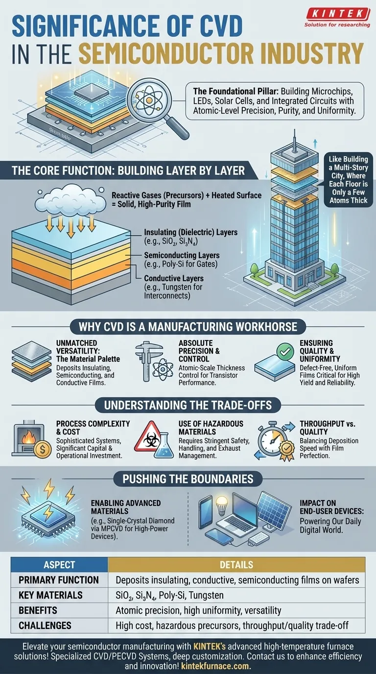
In the world of semiconductor manufacturing, Chemical Vapor Deposition (CVD) is not just one of many processes; it is a foundational pillar. It is the primary industrial method for depositing the ultra-thin, high-purity films of insulating, conductive, and semiconducting materials that form the intricate, multi-layered structures of integrated circuits (ICs), LEDs, and solar cells. Without CVD, the complex architecture of a modern microchip would be impossible to construct.
Building a microchip is like constructing a multi-story city where each floor is only a few atoms thick. CVD is the master construction technique, enabling engineers to build these layers with the atomic-level precision, purity, and uniformity required for modern electronics to function.
The Core Function: Building a Chip Layer by Layer
A modern semiconductor device is not a monolithic block but a three-dimensional marvel built from dozens or even hundreds of stacked layers on a silicon wafer. CVD is the process that creates many of these critical layers.
What is Thin Film Deposition?
Thin film deposition is the process of applying a very thin layer of material, often ranging from a few atoms to several micrometers thick, onto a substrate—in this case, the silicon wafer. Each film serves a specific electronic purpose.
How CVD Achieves This
CVD introduces reactive gases (precursors) into a chamber containing the wafer. These gases react or decompose on the wafer's heated surface, leaving behind a solid, high-purity film. The key to CVD's significance is its extraordinary level of control over this process.
Why CVD is a Manufacturing Workhorse
CVD's indispensability comes from its unique combination of versatility, precision, and the quality of the films it produces. It is used at multiple, critical stages of chip fabrication.
Unmatched Versatility: The Material Palette
CVD is not limited to one type of material. It is used to deposit the three fundamental categories of materials needed for a functional circuit.
- Insulating (Dielectric) Layers: Films like silicon dioxide (SiO₂) and silicon nitride (Si₃N₄) are deposited to electrically isolate different components from each other, preventing short circuits.
- Semiconducting Layers: Polycrystalline silicon (poly-Si) is a key material deposited via CVD to form the "gates" that turn transistors on and off.
- Conductive Layers: CVD is used to deposit metals like tungsten to create the microscopic wiring (interconnects) that connects the millions of transistors on a chip.
Absolute Precision and Control
The performance of a transistor is dictated by the exact thickness and properties of its constituent layers. CVD allows manufacturers to control film thickness with atomic-scale precision, ensuring that every transistor on the chip performs as designed.
Ensuring Quality and Uniformity
CVD produces films that are incredibly uniform and free of defects across the entire surface of the wafer. This uniformity is critical for achieving high manufacturing yields and ensuring the reliability and performance of the final device.
Understanding the Trade-offs
While indispensable, CVD is a complex and resource-intensive process. Objectivity requires acknowledging its inherent challenges.
Process Complexity and Cost
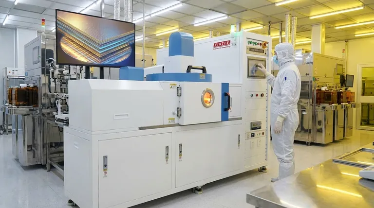
CVD systems are sophisticated, high-cost furnaces that require precise control over temperature, pressure, and gas flow. They represent a significant capital investment and operational expense in any semiconductor fabrication plant.
Use of Hazardous Materials
The chemical precursors used in CVD are often toxic, flammable, or corrosive. This necessitates stringent safety protocols, handling procedures, and exhaust management systems, adding to the overall complexity and cost of fabrication.
Throughput vs. Quality
There is often a trade-off between the speed of deposition (throughput) and the quality of the resulting film. Faster deposition can sometimes introduce imperfections, so engineers must constantly balance the need for high-quality films with the economic pressure for high-volume production.
Pushing the Boundaries of Electronics
CVD is not just a legacy technology; it is crucial for developing next-generation devices that demand materials with extreme properties.
Enabling Advanced Materials
Specialized techniques like Microwave Plasma CVD (MPCVD) are used to grow single-crystal diamond films. With exceptional thermal conductivity and electrical properties, these films enable high-frequency, high-power electronic devices for advanced telecommunications and computing.
Impact on End-User Devices
The quality of CVD processes directly translates to the performance of devices we use daily. From the ICs in our smartphones and televisions to the efficiency of solar panels and the brightness of LEDs, the foundation was laid by CVD.
How to Contextualize the Role of CVD
Your perspective on CVD's significance depends on your specific focus within the industry.
- If your primary focus is device fabrication: View CVD as the essential architectural tool used to build the core structures of transistors and the insulating and connecting layers that make them function as a circuit.
- If your primary focus is materials science: See CVD as a versatile synthesis method for creating high-purity, crystalline thin films with precisely tailored electronic, optical, and mechanical properties.
- If your primary focus is system performance: Understand that the quality of CVD deposition directly impacts the final chip's speed, power efficiency, and long-term reliability.
Ultimately, mastering CVD is fundamental to mastering the art of building the microscopic foundations upon which our entire digital world is built.
Summary Table:
| Aspect | Details |
|---|---|
| Primary Function | Deposits insulating, conductive, and semiconducting thin films on silicon wafers |
| Key Materials | Silicon dioxide (SiO₂), silicon nitride (Si₃N₄), polycrystalline silicon (poly-Si), tungsten |
| Benefits | Atomic-scale precision, high uniformity, versatility in material deposition |
| Applications | Integrated circuits (ICs), LEDs, solar cells, advanced electronics |
| Challenges | High cost, use of hazardous precursors, throughput vs. quality trade-offs |
Elevate your semiconductor manufacturing with KINTEK's advanced high-temperature furnace solutions! Leveraging exceptional R&D and in-house manufacturing, we provide diverse laboratories with precision tools like CVD/PECVD Systems, Muffle, Tube, and Rotary Furnaces, tailored to your unique experimental needs. Our strong deep customization capability ensures optimal performance for your thin film deposition processes. Contact us today to discuss how we can enhance your production efficiency and innovation!
Visual Guide
Related Products
- Custom Made Versatile CVD Tube Furnace Chemical Vapor Deposition CVD Equipment Machine
- MPCVD Machine System Reactor Bell-jar Resonator for Lab and Diamond Growth
- Multi Heating Zones CVD Tube Furnace Machine for Chemical Vapor Deposition Equipment
- 915MHz MPCVD Diamond Machine Microwave Plasma Chemical Vapor Deposition System Reactor
- Slide PECVD Tube Furnace with Liquid Gasifier PECVD Machine
People Also Ask
- What future trends are expected in the development of CVD tube furnaces? Discover Smarter, More Versatile Systems
- What are the benefits of developing new precursor materials for CVD tube furnaces? Unlock Advanced Thin-Film Synthesis
- What is a CVD tube furnace and what is its primary function? Discover Precision Thin-Film Deposition
- How does CVD tube furnace sintering enhance graphene growth? Achieve Superior Crystallinity and High Electron Mobility
- What improvements can be made to the bonding force of gate dielectric films using a CVD tube furnace? Enhance Adhesion for Reliable Devices


