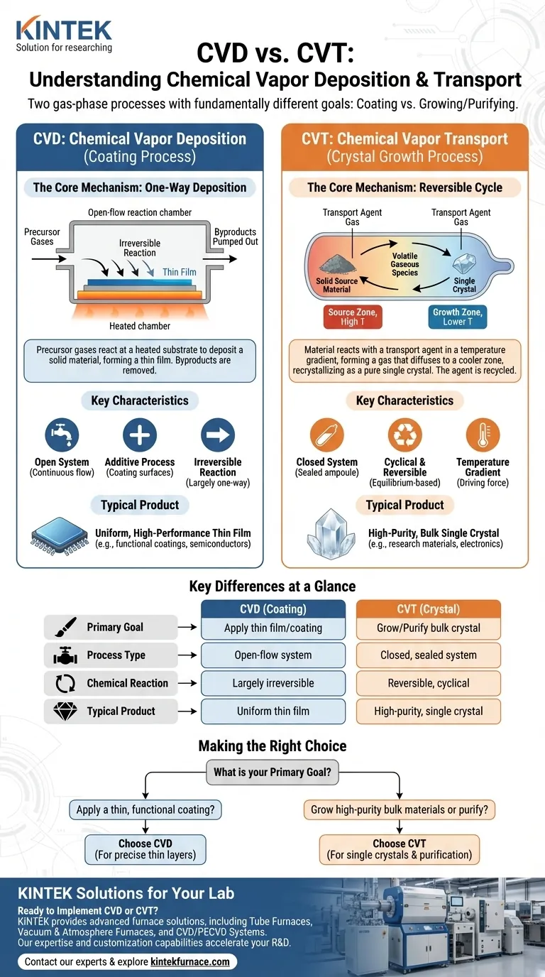
While both processes utilize chemical reactions in the gas phase, they serve fundamentally different purposes. Chemical Vapor Deposition (CVD) is a technique used to apply a thin film or coating onto a substrate, while Chemical Vapor Transport (CVT) is a method used to grow bulk, single crystals of a material or to purify it. They are distinct processes in their mechanism, setup, and final product.
The core distinction lies in their objective. CVD is an additive, one-way deposition process designed for coating surfaces. CVT is a cyclical, reversible transport process designed for growing and purifying bulk materials from one location to another.
Unpacking Chemical Vapor Deposition (CVD): The Coating Process
CVD is an essential technique in industries like semiconductor manufacturing and materials engineering where surface properties are critical. The goal is always to add a new layer to an existing object.
The Core Mechanism: One-Way Deposition
In CVD, one or more volatile precursor gases are introduced into a reaction chamber, typically under vacuum. These gases are not the final material itself, but rather molecules that contain the required atoms.
The gases flow over a heated substrate. The thermal energy at the substrate's surface causes the precursor gases to decompose or react with each other.
This reaction results in the deposition of a solid material, atom-by-atom or molecule-by-molecule, directly onto the substrate's surface, forming a thin, solid film. Any unreacted gases and byproducts are pumped out of the system.
The Outcome: A High-Performance Thin Film
The end result of CVD is a highly uniform, dense, and durable coating. The properties of this film—such as its thickness, composition, and crystal structure—can be precisely controlled by adjusting process parameters like temperature, pressure, and gas flow rates.
Common Applications
CVD is widely used to create functional coatings. This includes the silicon layers in microchips, wear-resistant diamond-like carbon coatings on cutting tools, and anti-reflective coatings on optics.
Understanding Chemical Vapor Transport (CVT): The Crystal Growth Process
CVT operates on a completely different principle. It isn't about coating a foreign substrate but about moving and recrystallizing a material that you already have in a solid, often polycrystalline, form.
The Core Mechanism: A Reversible Cycle
The process typically occurs within a sealed, evacuated quartz tube (an ampoule) that contains the source material (e.g., a powder) and a small amount of a "transport agent" gas.
This sealed tube is placed in a furnace with a temperature gradient, meaning one end is hotter than the other.
At the hot end (the source zone), the solid material reacts with the transport agent to form a new, volatile gaseous species. This gaseous molecule then diffuses to the colder end of the tube (the growth zone).
The Driving Force: The Temperature Gradient
In the cooler growth zone, the chemical reaction reverses. The gaseous molecule becomes unstable and decomposes, redepositing the original material—but now in a highly ordered, single-crystal form. The freed-up transport agent gas then diffuses back to the hot zone to pick up more material, repeating the cycle.
The Outcome: A High-Purity Bulk Crystal
The result of CVT is not a thin film, but a high-purity, often beautifully faceted, single crystal. The slow, controlled nature of the process allows atoms to arrange themselves perfectly, which is ideal for fundamental research and specialized electronic applications.
Key Differences at a Glance
The choice between CVD and CVT comes down to a fundamental difference in goals. One is for coating, the other for growing.
Objective: Coating vs. Growing
CVD is an additive manufacturing process. Its sole purpose is to add a thin layer of a new material onto a substrate.
CVT is a purification and recrystallization process. Its purpose is to take a solid material and regrow it elsewhere in a more perfect crystalline form.
Process Type: Open vs. Closed System
CVD is typically an open-flow system. Precursor gases continuously flow into the chamber and byproducts are continuously pumped out.
CVT is almost always a closed system. The material and transport agent are sealed within a tube, and the transport agent is recycled internally throughout the process.
Chemical Reaction: Irreversible vs. Reversible
The reactions in CVD are designed to be largely irreversible on the substrate surface. The goal is for the material to deposit and stay there.
The entire principle of CVT relies on a reversible chemical equilibrium that proceeds in one direction at a high temperature and in the opposite direction at a lower temperature.
Making the Right Choice for Your Goal
Selecting the correct method requires a clear understanding of your desired outcome.
- If your primary focus is to apply a thin, functional, or protective coating onto a component: CVD is the appropriate technique for depositing layers with precisely controlled properties.
- If your primary focus is to grow high-purity, single-crystal materials for research or specialized electronics: CVT is the established method for this purpose, starting from a polycrystalline powder.
- If your primary focus is to purify an existing solid material: CVT can be used to physically separate the desired material from non-volatile impurities by transporting it to a different location within the ampoule.
Ultimately, understanding whether you need to coat a surface or grow a bulk material is the definitive factor in choosing between these two powerful techniques.
Summary Table:
| Feature | Chemical Vapor Deposition (CVD) | Chemical Vapor Transport (CVT) |
|---|---|---|
| Primary Goal | Apply a thin film/coating onto a substrate | Grow/purify bulk, single-crystal materials |
| Process Type | Open-flow system | Closed, sealed system |
| Chemical Reaction | Largely irreversible | Reversible, cyclical |
| Typical Product | Uniform thin film on a foreign substrate | High-purity, single crystal |
| System Setup | Reaction chamber with gas flow | Sealed ampoule in a temperature gradient furnace |
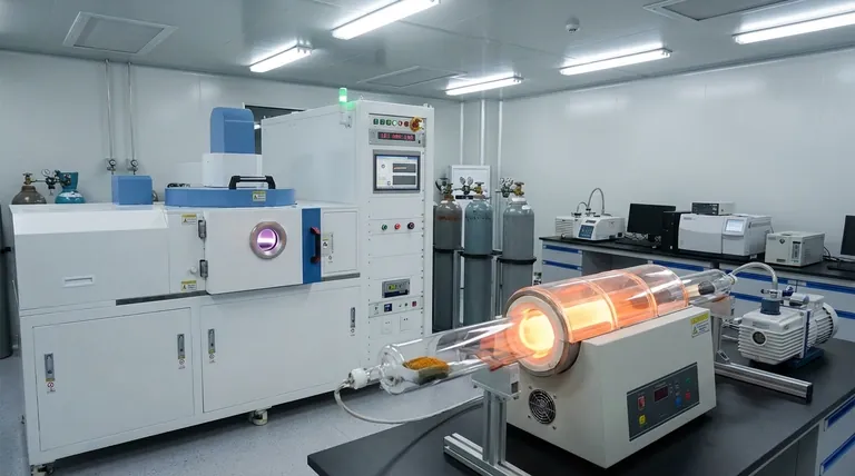
Ready to Implement CVD or CVT in Your Lab?
Choosing the right high-temperature processing equipment is critical for successful thin-film deposition or crystal growth. KINTEK leverages exceptional R&D and in-house manufacturing to provide diverse laboratories with advanced furnace solutions tailored for these precise applications.
Our product line, including Tube Furnaces, Vacuum & Atmosphere Furnaces, and CVD/PECVD Systems, is complemented by strong deep customization capabilities to precisely meet your unique experimental requirements, whether you are developing new semiconductor coatings or growing research-grade single crystals.
Let's discuss your project needs and explore how our expertise can accelerate your research and development.
Contact our experts today to request a consultation
Visual Guide
Related Products
- Custom Made Versatile CVD Tube Furnace Chemical Vapor Deposition CVD Equipment Machine
- Slide PECVD Tube Furnace with Liquid Gasifier PECVD Machine
- Multi Heating Zones CVD Tube Furnace Machine for Chemical Vapor Deposition Equipment
- MPCVD Machine System Reactor Bell-jar Resonator for Lab and Diamond Growth
- RF PECVD System Radio Frequency Plasma Enhanced Chemical Vapor Deposition
People Also Ask
- How does CVD tube furnace sintering enhance graphene growth? Achieve Superior Crystallinity and High Electron Mobility
- What are the key application fields of CVD tube furnaces? Unlock Precision in Thin-Film Synthesis
- How might AI and machine learning enhance CVD tube furnace processes? Boost Quality, Speed, and Safety
- How can integrating CVD tube furnaces with other technologies benefit device fabrication? Unlock Advanced Hybrid Processes
- Why are CVD tube furnace sintering systems indispensable for 2D material research and production? Unlock Atomic-Scale Precision


