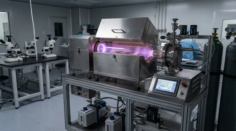
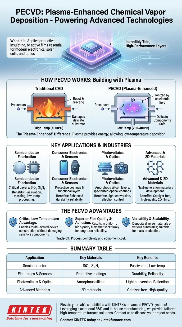
At its core, Plasma-Enhanced Chemical Vapor Deposition (PECVD) is used to apply incredibly thin, high-performance layers of material onto a surface. These films are essential for manufacturing a vast range of modern technologies, including semiconductors, solar cells, consumer electronics like smartphones, and advanced optical components. The process uses an energized gas, or plasma, to deposit materials like silicon dioxide and silicon nitride, creating protective, insulating, or electronically active layers.
The fundamental advantage of PECVD is its ability to deposit high-quality, uniform films at low temperatures. This makes it the go-to process for building complex devices where high heat would damage the underlying sensitive components.
How PECVD Works: Building with Plasma
PECVD is a refined form of chemical vapor deposition (CVD). Understanding its unique mechanism reveals why it's so critical for high-tech manufacturing.
The Basic Deposition Process
In any CVD process, precursor gases are introduced into a chamber containing the object to be coated, known as the substrate. A chemical reaction is triggered, causing a solid material to form and deposit as a thin film onto that substrate.
The "Plasma-Enhanced" Difference
Traditional CVD requires very high temperatures (often over 600°C) to provide the energy needed for the chemical reaction. PECVD bypasses this requirement by using an electric field to ionize the gas, creating a plasma.
This plasma provides the energy for the reaction, allowing the deposition to occur at much lower temperatures (typically 200-400°C). This is the key that unlocks its use in modern electronics.
Key Applications and Industries
PECVD's unique capabilities make it indispensable across several high-value industries. It enables the creation of layers ranging from a few angstroms to several micrometers thick.
Semiconductor Fabrication
This is the largest application of PECVD. It is used to deposit critical layers like silicon dioxide (SiO₂) and silicon nitride (Si₃N₄).
These films serve as high-quality passivation layers, which protect the sensitive semiconductor device from moisture and contamination, and as high-density masks that define circuit patterns.
Consumer Electronics and Sensors
Nearly every complex electronic device contains components made with PECVD. This includes smartphones, wearables, and automotive sensors.
The process creates protective coatings that enhance durability and reliability, as well as functional layers within the sensors themselves.
Photovoltaics and Optics
In solar cells, PECVD is used to deposit layers of amorphous silicon, which are vital for converting sunlight into electricity.
It is also used to create specialized optical coatings on lenses and other components, controlling reflection, absorption, and transmission of light.
Advanced and 2D Materials
Researchers use PECVD to develop next-generation materials. Its low-temperature, catalyst-free nature makes it ideal for preparing high-quality 2D materials, which have novel electronic and physical properties.
Understanding the Trade-offs: The Advantages of PECVD
Choosing a deposition method is a matter of balancing cost, quality, and material constraints. PECVD's trade-offs make it a superior choice for many demanding applications.
The Critical Low-Temperature Advantage
The primary reason to choose PECVD is its low operating temperature. Fabricating a modern microchip involves building dozens of layers. High-temperature processes would destroy the delicate circuitry already built in the lower layers. PECVD's low-temperature nature makes this complex, multi-layered construction possible.
Superior Film Quality and Adhesion
The plasma-driven process results in films that are highly uniform, meaning the thickness is consistent across the entire substrate. The films also exhibit exceptional purity and adhesion, sticking firmly to the substrate for long-term reliability.
Versatility and Scalability
PECVD is highly versatile, capable of depositing a wide variety of film compositions onto substrates of different materials and complex geometries. The process is well-established, reliable, and efficient, making it suitable for large-scale, cost-effective manufacturing.
Acknowledging the Complexity
The main trade-off is process complexity. Managing a stable plasma requires sophisticated and expensive equipment. While scalable and cost-effective for mass production, the initial capital investment is significant compared to simpler deposition techniques.
Making the Right Choice for Your Goal
Selecting PECVD depends entirely on the requirements of your final product. The decision hinges on balancing film performance with thermal and budget constraints.
- If your primary focus is manufacturing sensitive electronics or multi-layered devices: PECVD is the industry standard, as its low-temperature process prevents damage to delicate underlying components.
- If your primary focus is creating highly durable, pure, and uniform protective coatings at scale: PECVD offers a reliable and repeatable method for producing high-quality passivation films for everything from microchips to sensors.
- If your primary focus is compatibility with a wide range of materials and geometries: The versatility of PECVD allows for excellent film deposition on various substrates, making it a flexible solution for advanced R&D and manufacturing.
Ultimately, PECVD is a cornerstone technology that enables the precision and performance required by the world's most advanced electronic and optical devices.
Summary Table:
| Application | Key Materials Deposited | Key Benefits |
|---|---|---|
| Semiconductor Fabrication | Silicon Dioxide (SiO₂), Silicon Nitride (Si₃N₄) | Passivation, masking, low-temperature processing |
| Consumer Electronics & Sensors | Protective coatings, functional layers | Durability, reliability, low heat damage |
| Photovoltaics & Optics | Amorphous silicon, optical coatings | Light conversion, reflection control |
| Advanced Materials | 2D materials | Catalyst-free, high-quality deposition |
Elevate your lab's capabilities with KINTEK's advanced PECVD systems! Leveraging exceptional R&D and in-house manufacturing, we provide diverse laboratories with tailored high-temperature furnace solutions, including CVD/PECVD Systems. Our strong deep customization capability ensures precise alignment with your unique experimental needs, enhancing efficiency and innovation. Contact us today to discuss how our solutions can benefit your projects!
Visual Guide
Related Products
- RF PECVD System Radio Frequency Plasma Enhanced Chemical Vapor Deposition
- Slide PECVD Tube Furnace with Liquid Gasifier PECVD Machine
- Inclined Rotary Plasma Enhanced Chemical Deposition PECVD Tube Furnace Machine
- Inclined Rotary Plasma Enhanced Chemical Deposition PECVD Tube Furnace Machine
- Cylindrical Resonator MPCVD Machine System for Lab Diamond Growth
People Also Ask
- What are the applications of plasma enhanced chemical vapor deposition? Key Uses in Electronics, Optics & Materials
- What are the advantages of PECVD in film deposition? Achieve Low-Temp, High-Quality Coatings
- What is PECVD specification? A Guide to Choosing the Right System for Your Lab
- What are some promising applications of PECVD-prepared 2D materials? Unlock Advanced Sensing and Optoelectronics
- What is RF in PECVD? A Critical Control for Plasma Deposition


