At its core, Microwave Plasma Chemical Vapor Deposition (MPCVD) is a method for growing high-quality synthetic diamonds by activating carbon-containing gas with microwaves. It is widely regarded as the superior technique compared to older methods like Hot Filament (HFCVD) or DC Plasma Jet CVD because it produces exceptionally pure diamonds with greater control and consistency over large areas.
While various methods can create lab-grown diamonds, MPCVD stands apart. Its unique ability to generate a clean, stable plasma without internal electrodes or filaments solves the core problems of contamination and instability that limit other techniques.
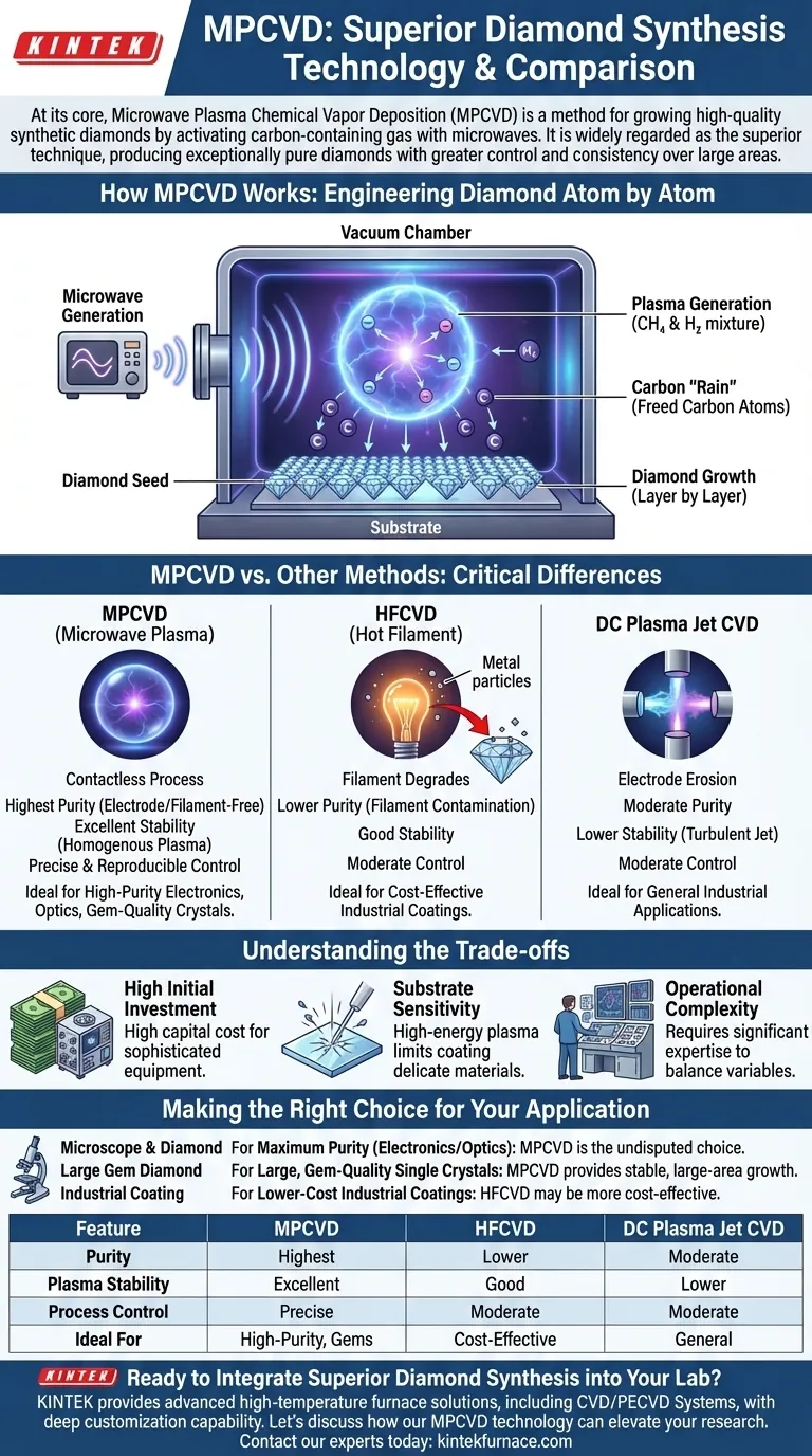
How MPCVD Works: Engineering Diamond Atom by Atom
To understand why MPCVD is so effective, you must first understand its fundamental process. It is a method of precision engineering, not brute force.
Generating Plasma with Microwaves
The process begins inside a vacuum chamber. A mixture of gases, typically methane (the source of carbon) and hydrogen, is introduced at very low pressure.
Microwaves are then directed into the chamber, energizing the gas and stripping electrons from the atoms. This creates a glowing ball of superheated, ionized gas known as plasma.
The Carbon "Rain"
Within this plasma, the methane molecules (CH₄) are broken apart. This frees up carbon atoms, which then "rain" down onto a substrate below.
This substrate is typically a small, high-quality diamond "seed." The carbon atoms land on the seed's crystal lattice and arrange themselves perfectly, causing the diamond to grow layer by layer.
MPCVD vs. Other Methods: The Critical Differences
The superiority of MPCVD is not a matter of opinion but a result of solving specific engineering challenges that plague other Chemical Vapor Deposition (CVD) methods.
The Purity Advantage (vs. HFCVD)
Hot Filament CVD (HFCVD) uses a heated metal wire, much like the filament in an old incandescent light bulb, to break down the carbon gas.
Over time, this filament degrades and sputters metal atoms (like tungsten) into the chamber. These atoms become trapped in the growing diamond, creating impurities that compromise its optical and electronic properties.
MPCVD is contactless. Because the plasma is generated by microwaves, there are no internal components to degrade, resulting in a significantly purer diamond.
The Stability Advantage (vs. DC Plasma Jet)
Other plasma-based methods, like DC Plasma Jet CVD, use an electrical discharge between two electrodes to create the plasma.
This can create a "jet" that is often turbulent and less uniform, leading to inconsistent growth rates and quality across the diamond's surface.
MPCVD generates a large, stable, and homogenous plasma ball. This stable environment is essential for growing large, single-crystal diamonds without internal stress or defects.
The Control Advantage
The MPCVD process allows for extremely precise and stable control over key variables like temperature, gas composition, and pressure.
This level of control means the diamond's properties can be tailored for specific applications, and the results are highly reproducible—a critical factor for any industrial-scale production.
Understanding the Trade-offs
No technology is without its limitations. Objectivity requires acknowledging where MPCVD falls short.
High Initial Investment
MPCVD systems are complex and require sophisticated microwave generators, vacuum pumps, and control systems. This results in a high capital cost for the equipment, making it less accessible than simpler setups like HFCVD.
Substrate Sensitivity
The high-energy plasma generated by the microwaves can be damaging to certain sensitive materials. This limits its use for coating delicate substrates, such as some polymers or organic materials.
Operational Complexity
Achieving optimal results requires significant expertise. Operators must carefully balance the intricate interplay of microwave power, gas flow, and chamber pressure to maintain stable growth conditions.
Making the Right Choice for Your Application
Your choice of synthesis method depends entirely on your end goal. The trade-offs between quality, cost, and scalability define the decision.
- If your primary focus is maximum purity for electronic or optical use: MPCVD is the undisputed choice due to its contamination-free process.
- If your primary focus is growing large, gem-quality single crystals: MPCVD provides the stable, large-area plasma necessary for consistent and flawless growth.
- If your primary focus is lower-cost industrial coatings where minor impurities are acceptable: A simpler method like HFCVD may be a more cost-effective solution.
Ultimately, MPCVD represents a pivotal shift towards precision atomic-level manufacturing, enabling a new generation of high-performance materials.
Summary Table:
| Feature | MPCVD | HFCVD (Hot Filament) | DC Plasma Jet CVD |
|---|---|---|---|
| Purity | Highest (Electrode/ Filament-Free) | Lower (Filament Contamination) | Moderate (Electrode Erosion) |
| Plasma Stability | Excellent (Stable, Homogenous Plasma Ball) | Good | Lower (Turbulent Jet) |
| Process Control | Precise & Reproducible | Moderate | Moderate |
| Ideal For | High-Purity Electronics, Optics, Gem-Quality Crystals | Cost-Effective Industrial Coatings | General Industrial Applications |
| Key Limitation | High Equipment Cost & Operational Complexity | Lower Purity | Less Uniform Growth |
Ready to Integrate Superior Diamond Synthesis into Your Lab?
Leveraging exceptional R&D and in-house manufacturing, KINTEK provides diverse laboratories with advanced high-temperature furnace solutions. Our product line, including Muffle, Tube, Rotary Furnaces, Vacuum & Atmosphere Furnaces, and specialized CVD/PECVD Systems, is complemented by our strong deep customization capability to precisely meet your unique experimental requirements—whether you're developing next-generation semiconductors, advanced optics, or high-performance materials.
Let's discuss how our MPCVD technology and expertise can elevate your research and production. Contact our experts today for a tailored solution.
Visual Guide
Related Products
- 915MHz MPCVD Diamond Machine Microwave Plasma Chemical Vapor Deposition System Reactor
- MPCVD Machine System Reactor Bell-jar Resonator for Lab and Diamond Growth
- Cylindrical Resonator MPCVD Machine System for Lab Diamond Growth
- Multi Heating Zones CVD Tube Furnace Machine for Chemical Vapor Deposition Equipment
- Inclined Rotary Plasma Enhanced Chemical Deposition PECVD Tube Furnace Machine
People Also Ask
- What is the basic principle of operation for the microwave plasma chemical vapor deposition system? Unlock High-Purity Material Growth
- What is the purpose of a microwave plasma chemical vapor deposition system? Grow High-Purity Diamonds and Advanced Materials
- How does the MPCVD process work to deposit diamond? A Guide to High-Purity Synthesis
- What are the essential components of an MPCVD reactor for diamond film deposition? Unlock High-Quality Diamond Growth
- In which industries is the microwave plasma chemical vapor deposition system commonly used? Unlock High-Purity Material Synthesis


