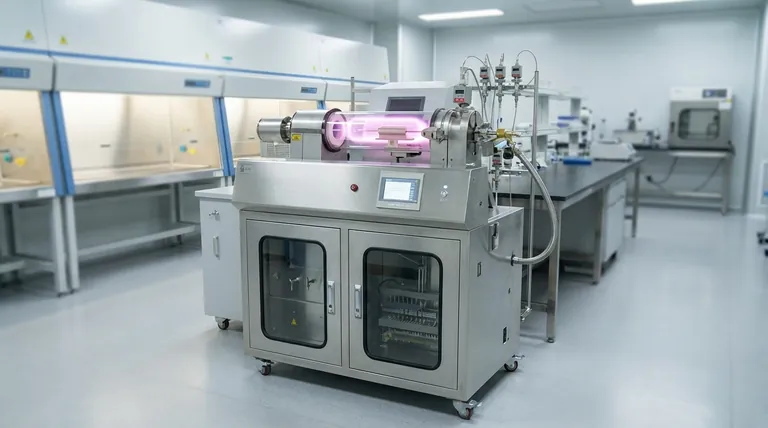
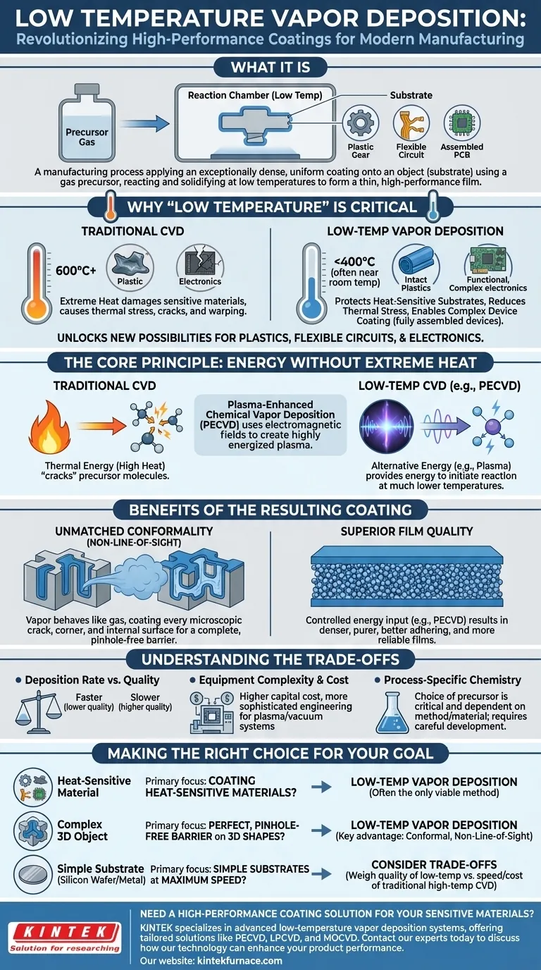
At its core, low-temperature vapor deposition is a manufacturing process used to apply an exceptionally dense and uniform coating onto an object, or "substrate." It achieves this by turning a chemical precursor into a gas, which then reacts and solidifies on the substrate's surface, forming a thin, high-performance film without requiring the extreme heat of traditional methods.
This technology's crucial advantage is its ability to coat heat-sensitive materials. It enables the application of protective, high-performance films on modern products like plastics, flexible circuits, and complex assembled electronics that would be damaged or destroyed by conventional high-temperature coating processes.
Why "Low Temperature" is a Critical Advantage
Traditional Chemical Vapor Deposition (CVD) often requires temperatures exceeding 600°C (1112°F). Low-temperature variants operate significantly cooler, often below 400°C and sometimes near room temperature, unlocking new manufacturing possibilities.
Protecting Sensitive Substrates
Many modern materials simply cannot withstand high heat. Plastics would melt, and the delicate components inside a smartphone or sensor would be irreparably damaged. Low-temperature processes make it possible to coat these materials directly.
Reducing Thermal Stress
Even for materials that can survive high temperatures, the process of heating and cooling can introduce mechanical stress. This stress can cause the substrate to warp or lead to cracks and delamination in the coating itself, compromising its integrity.
Enabling Complex Device Manufacturing
Low-temperature deposition allows for coating fully or partially assembled devices. Instead of coating individual components and then assembling them, manufacturers can apply a final protective layer over an entire electronic assembly, simplifying production and ensuring comprehensive protection.
The Core Principle: Energy Without Extreme Heat
The fundamental challenge is providing enough energy to drive the chemical reaction without relying on intense heat.
Standard CVD: Thermal Energy
In traditional CVD, high temperature is the energy source. It thermally "cracks" the precursor gas molecules, causing them to break apart and react to form the desired film on the substrate.
Low-Temp CVD: Alternative Energy Sources
Low-temperature methods substitute heat with other forms of energy. The most common method is Plasma-Enhanced Chemical Vapor Deposition (PECVD), which uses an electromagnetic field (like radio frequency or microwave) to create a plasma.
This plasma, a highly energized state of gas, provides the energy needed to initiate the chemical reaction at a much lower temperature.
Benefits of the Resulting Coating
The value of this process lies not only in its compatibility with sensitive materials but also in the quality of the film it produces.
Unmatched Conformality (Non-Line-of-Sight)
Vapor deposition creates a conformal coating. Unlike a spray paint that only covers what it can "see" (line-of-sight), the vapor precursor behaves like a gas, flowing into and coating every microscopic crack, corner, and internal surface. This creates a truly complete, pinhole-free barrier.
Superior Film Quality
The controlled energy input from methods like PECVD often results in films that are denser, purer, and have better adhesion than those from other processes. This leads to more reliable and durable performance.
Understanding the Trade-offs
While powerful, low-temperature deposition is not a universal solution. It involves specific engineering trade-offs.
Deposition Rate vs. Quality
Generally, low-temperature processes can be slower than their high-temperature counterparts. There is often a trade-off between the speed of coating deposition and the final quality and uniformity of the film.
Equipment Complexity and Cost
Systems for processes like PECVD are more complex and carry a higher capital cost than simple thermal CVD furnaces. The use of plasma and vacuum systems requires more sophisticated engineering and maintenance.
Process-Specific Chemistry
The choice of precursor chemicals is critical and highly dependent on the specific deposition method and desired film material. Not all materials can be easily deposited using low-temperature techniques, requiring careful process development.
Making the Right Choice for Your Goal
Selecting the right coating technology depends entirely on your material, product complexity, and performance requirements.
- If your primary focus is coating heat-sensitive materials like plastics or assembled electronics: Low-temperature vapor deposition is not just an option; it is often the only viable high-performance method.
- If your primary focus is achieving a perfect, pinhole-free barrier on a complex 3D shape: The conformal, "non-line-of-sight" nature of vapor deposition is your key advantage, and low-temp processes make this available for a wider range of products.
- If your primary focus is coating simple, robust substrates (like silicon wafers or metals) at maximum speed: You must weigh the superior film quality of low-temp methods against the potentially faster rates and lower equipment cost of traditional high-temperature CVD.
Ultimately, low-temperature vapor deposition transforms high-performance coatings from a specialized industrial process into a versatile tool for innovation across countless modern products.
Summary Table:
| Key Feature | Benefit |
|---|---|
| Low-Temperature Operation (often <400°C) | Protects heat-sensitive substrates like plastics and assembled electronics |
| Conformal Coating | Covers complex 3D shapes, cracks, and internal surfaces uniformly |
| Superior Film Quality | Creates dense, pinhole-free barriers with excellent adhesion |
| Enables Complex Manufacturing | Allows coating of fully assembled devices for comprehensive protection |
Need a high-performance coating solution for your sensitive materials? KINTEK specializes in advanced low-temperature vapor deposition systems. Leveraging our exceptional R&D and in-house manufacturing, we provide diverse laboratories with tailored solutions like our PECVD, LPCVD, and MOCVD systems. Our strong deep customization capability ensures we can precisely meet your unique experimental and production requirements. Contact our experts today to discuss how our technology can enhance your product performance and manufacturing process.
Visual Guide
Related Products
- HFCVD Machine System Equipment for Drawing Die Nano Diamond Coating
- Custom Made Versatile CVD Tube Furnace Chemical Vapor Deposition CVD Equipment Machine
- Multi Heating Zones CVD Tube Furnace Machine for Chemical Vapor Deposition Equipment
- MPCVD Machine System Reactor Bell-jar Resonator for Lab and Diamond Growth
- 915MHz MPCVD Diamond Machine Microwave Plasma Chemical Vapor Deposition System Reactor
People Also Ask
- What is chemical vapor deposition (CVD) and its primary industrial application? Unlock Precision Thin Films for Electronics
- What materials are commonly used in CVD coating systems? Explore Key Materials for Superior Coatings
- What role does Chemical Vapor Deposition (CVD) equipment play in the surface coating of carbon fibers for composites?
- What core function does CVD equipment serve in h-BN anti-corrosion? Master Precision Synthesis for High-Performance Films
- What is the advantage of using a CVD system for coating turbine blades? Master Complex Geometries with Ease


