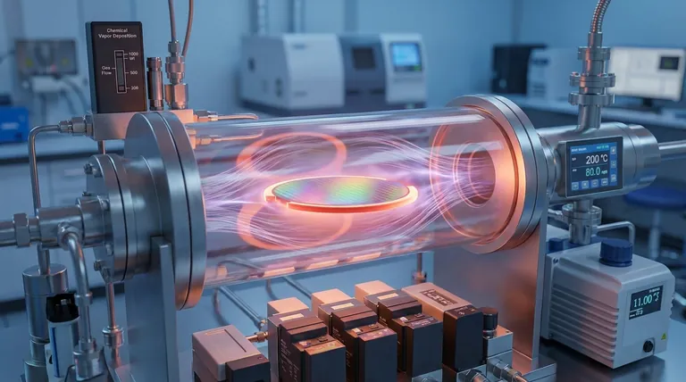
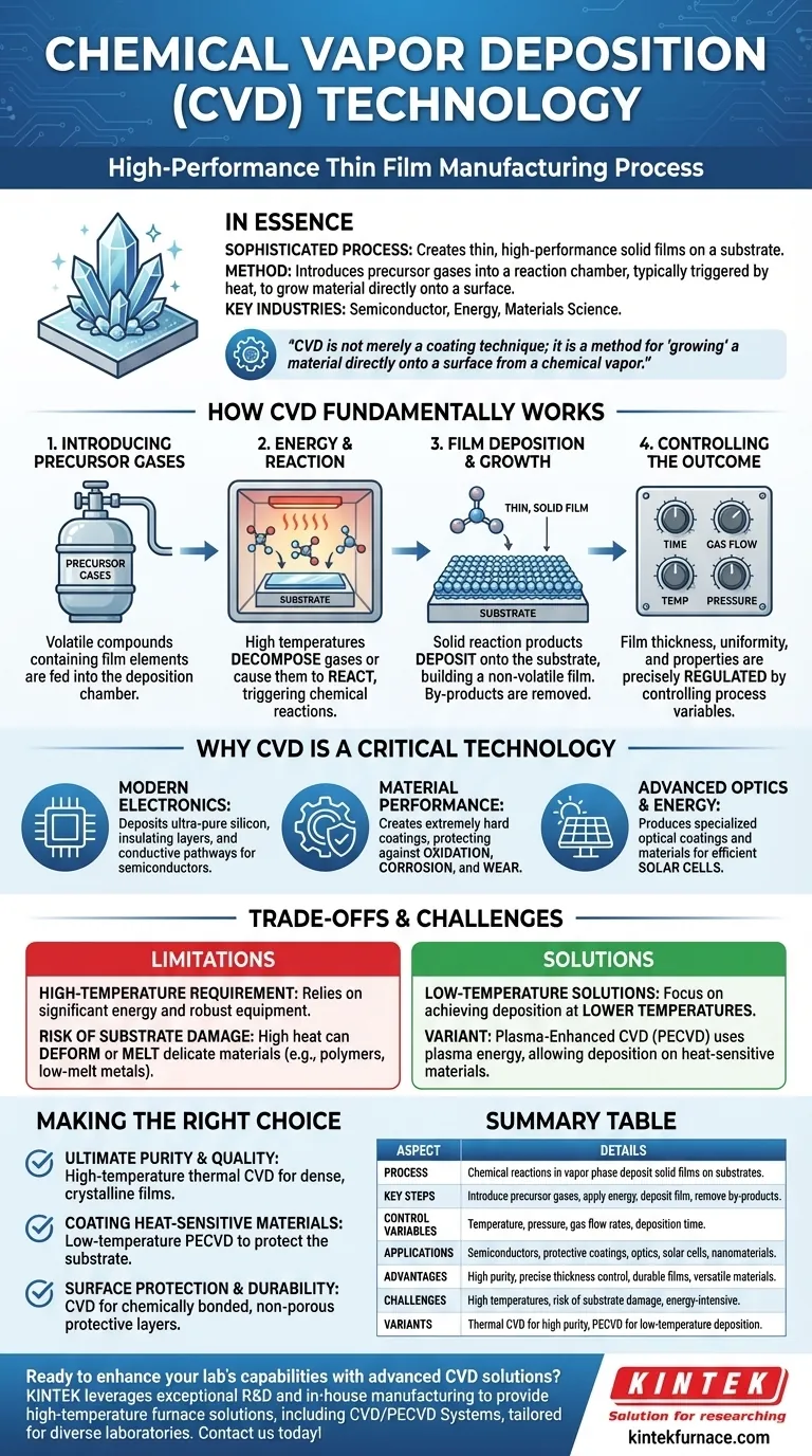
In essence, Chemical Vapor Deposition (CVD) is a sophisticated manufacturing process used to create thin, high-performance solid films on a surface, known as a substrate. It achieves this by introducing precursor gases into a reaction chamber, where chemical reactions are triggered—typically by heat—causing a solid material to form and deposit onto the substrate. This method is fundamental to producing the high-purity, durable coatings required by the semiconductor, energy, and materials science industries.
At its core, CVD is not merely a coating technique; it is a method for "growing" a material directly onto a surface from a chemical vapor. This precise, bottom-up approach allows for exceptional control over a film's thickness, composition, and structural properties.
How CVD Fundamentally Works
The CVD process can be broken down into a few critical steps that transform gas into a solid, functional film. It is a highly controlled thermochemical process.
Introducing Precursor Gases
The process begins by feeding one or more volatile precursor gases into a deposition chamber, which is often held under a vacuum or at atmospheric pressure. These precursors are chemical compounds that contain the elements required for the final film.
The Role of Energy and Reaction
The chamber and the substrate within it are heated to very high temperatures. This thermal energy breaks down (decomposes) the precursor gases or causes them to react with one another. This chemical reaction is the heart of the CVD process.
Film Deposition and Growth
The solid products from this chemical reaction then deposit onto all exposed surfaces of the substrate. This deposition occurs atom by atom or molecule by molecule, building up a thin, solid, and non-volatile film. Unreacted gases and chemical by-products are continuously removed from the chamber.
Controlling the Outcome
The final properties of the film are not accidental. Engineers precisely regulate the film’s thickness and uniformity by controlling key variables like the deposition time, gas concentration and flow rates, temperature, and pressure.
Why CVD is a Critical Technology
CVD is not an obscure laboratory technique; it is a cornerstone of modern high-tech manufacturing, enabling products that define our daily lives.
Building Modern Electronics
CVD is indispensable in semiconductor manufacturing. It is used to deposit the ultra-pure silicon films, insulating layers (like silicon nitride), and conductive pathways that form the basis of microchips and processors.
Enhancing Material Performance
The process creates extremely hard and durable protective coatings. These films are applied to mechanical parts, tools, and other components to protect them from oxidation, corrosion, and wear, dramatically extending their operational lifespan.
Powering Advanced Optics and Energy
In optoelectronics, CVD is used to create specialized optical coatings for lenses and to produce the high-purity materials essential for efficient solar cells and other light-sensitive devices.
Innovating in Science and Medicine
The precision of CVD makes it a vital tool for creating nanomaterials, specialized surfaces for analytical and life science instruments, and other high-performance materials where purity and durability are paramount.
Understanding the Trade-offs and Challenges
While incredibly powerful, the CVD process is not without its limitations. Understanding these trade-offs is key to its proper application.
The High-Temperature Requirement
Traditional CVD processes rely on very high temperatures to initiate the necessary chemical reactions. This requires a significant amount of energy and robust equipment.
Risk of Substrate Damage
The high heat can be a major problem. It can deform, melt, or change the internal structure of the substrate being coated, especially if that material is a polymer, a low-melting-point metal, or has a delicate structure. This limits the types of materials that can be coated with thermal CVD.
The Push for Low-Temperature Solutions
To overcome this limitation, a major focus of CVD development is on achieving deposition at lower temperatures. Variants like Plasma-Enhanced CVD (PECVD) use plasma instead of just heat to provide the energy for the reaction, allowing for high-quality films to be deposited on heat-sensitive materials.
Making the Right Choice for Your Goal
Selecting the right deposition approach depends entirely on your material and desired outcome.
- If your primary focus is ultimate purity and film quality: Traditional, high-temperature thermal CVD is often the best choice for creating dense, highly crystalline films for demanding applications like semiconductors.
- If your primary focus is coating heat-sensitive materials: A low-temperature variant like Plasma-Enhanced CVD (PECVD) is necessary to deposit a quality film without damaging the underlying substrate.
- If your primary focus is surface protection and durability: CVD is an excellent method for creating a chemically bonded, non-porous layer that offers superior protection against corrosion and wear.
Ultimately, Chemical Vapor Deposition is a foundational tool for engineering materials with atomic-level precision, enabling the performance required by our most advanced technologies.
Summary Table:
| Aspect | Details |
|---|---|
| Process | Chemical reactions in vapor phase deposit solid films on substrates. |
| Key Steps | Introduce precursor gases, apply energy (heat/plasma), deposit film, remove by-products. |
| Control Variables | Temperature, pressure, gas flow rates, deposition time. |
| Applications | Semiconductors, protective coatings, optics, solar cells, nanomaterials. |
| Advantages | High purity, precise thickness control, durable films, versatile materials. |
| Challenges | High temperatures, risk of substrate damage, energy-intensive. |
| Variants | Thermal CVD for high purity, PECVD for low-temperature deposition. |
Ready to enhance your lab's capabilities with advanced CVD solutions? KINTEK leverages exceptional R&D and in-house manufacturing to provide high-temperature furnace solutions, including CVD/PECVD Systems, tailored for diverse laboratories. Our deep customization ensures precise alignment with your unique experimental needs, from semiconductor production to material science innovations. Contact us today to discuss how our expertise can drive your projects forward with reliable, high-performance coatings!
Visual Guide
Related Products
- Custom Made Versatile CVD Tube Furnace Chemical Vapor Deposition CVD Equipment Machine
- Multi Heating Zones CVD Tube Furnace Machine for Chemical Vapor Deposition Equipment
- HFCVD Machine System Equipment for Drawing Die Nano Diamond Coating
- Split Chamber CVD Tube Furnace with Vacuum Station CVD Machine
- 915MHz MPCVD Diamond Machine Microwave Plasma Chemical Vapor Deposition System Reactor
People Also Ask
- Why are CVD tube furnace sintering systems indispensable for 2D material research and production? Unlock Atomic-Scale Precision
- How does CVD tube furnace sintering enhance graphene growth? Achieve Superior Crystallinity and High Electron Mobility
- What temperature range do standard CVD tube furnaces operate at? Unlock Precision for Your Material Deposition
- What are the practical applications of gate media prepared by CVD tube furnaces? Unlock Advanced Electronics and More
- What are the benefits of developing new precursor materials for CVD tube furnaces? Unlock Advanced Thin-Film Synthesis


