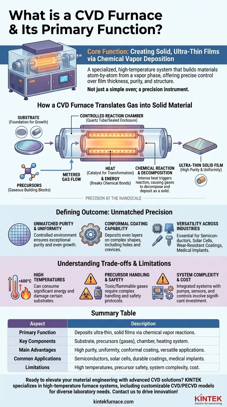
At its core, a Chemical Vapor Deposition (CVD) furnace is a highly specialized, high-temperature system engineered for a single primary function: to create a solid, ultra-thin film of material on the surface of a substrate. It accomplishes this not by melting or spraying, but by introducing carefully selected gases, known as precursors, into a controlled chamber. The furnace's intense heat then triggers a chemical reaction, causing these gases to decompose and deposit a uniform, high-purity solid layer onto the target object.
A CVD furnace should not be viewed as a simple oven. It is a precision instrument that enables engineers and scientists to construct materials atom-by-atom from a vapor phase, granting precise control over a film's thickness, purity, and structure.
How a CVD Furnace Translates Gas into Solid Material
The elegance of the CVD process lies in its ability to build a solid from the ground up. This transformation is orchestrated through several critical components and stages working in concert within the furnace.
The Substrate: The Foundation for Growth
The substrate is the base material or object onto which the new film is grown. This could be a silicon wafer for a microchip, a glass panel for a solar cell, or a metal tool bit that needs a hard coating. The furnace's role is to heat this substrate to the precise temperature required for the reaction.
The Precursors: The Gaseous Building Blocks
Precursors are chemical compounds that contain the elements you want to deposit. They are chosen because they can exist as a gas or vapor at manageable temperatures and will chemically react in a predictable way when heated. These gases are carefully metered and injected into the furnace chamber.
The Chamber: A Controlled Reaction Environment
The entire process takes place inside a sealed chamber, often a quartz tube in laboratory-scale systems. This enclosure is critical for maintaining an ultra-pure environment and controlling the atmosphere, pressure, and gas flow, preventing contamination and ensuring the chemical reaction proceeds as intended.
The Heat: The Catalyst for Transformation
Heat is the engine of the CVD process. The furnace raises the temperature of the substrate and the surrounding precursor gases, providing the necessary energy to break chemical bonds. This decomposition or reaction causes the desired solid material to "precipitate" out of the gas phase and deposit onto the hot substrate surface, forming a stable thin film.
The Defining Outcome: Precision at the Nanoscale
The reason CVD is indispensable in advanced manufacturing is not just that it creates films, but the quality of the films it creates. The process offers a level of control that is difficult to achieve with other methods.
Unmatched Purity and Uniformity
Because the precursors are delivered as high-purity gases and the reaction occurs in a controlled vacuum or specific atmosphere, the resulting films are exceptionally pure. The nature of the gas-phase reaction also allows the film to grow with remarkable uniformity across the entire substrate surface.
Conformal Coating Capability
A key advantage of CVD is its ability to create conformal coatings. This means the film deposits evenly over complex, three-dimensional shapes, covering surfaces inside holes and crevices just as well as it covers flat areas. This is vital for coating intricate components like those found in microelectronics.
Versatility Across Industries
This precise control makes CVD essential for a wide range of applications. It is the backbone of the semiconductor industry for building microchips, critical for producing high-efficiency solar cells, and used to apply wear-resistant coatings on cutting tools and medical implants.
Understanding the Trade-offs and Limitations
While powerful, the CVD process is not without its challenges. Understanding these trade-offs is key to appreciating its role and requirements.
The Need for High Temperatures
Many CVD processes require very high temperatures (often >600°C), which consumes significant energy. More importantly, these temperatures can damage or fundamentally alter certain substrate materials, limiting which substrates can be used for a given process.
Precursor Handling and Safety
The gaseous precursors used in CVD are often toxic, flammable, or corrosive. This necessitates complex gas handling and delivery systems, along with rigorous safety protocols and exhaust management, adding to the system's complexity and operational cost.
System Complexity and Cost
A CVD furnace is far more than a heating element in a box. It is an integrated system involving vacuum pumps, mass flow controllers for precise gas metering, pressure sensors, and sophisticated control software. This complexity makes industrial-scale CVD systems a significant capital investment.
How to Apply This to Your Project
Your choice of CVD furnace and process is dictated entirely by your end goal and the materials you are working with.
- If your primary focus is foundational research or new material discovery: A versatile, modular laboratory-scale tube furnace offers the flexibility needed to experiment with different precursors, temperatures, and substrates.
- If your primary focus is semiconductor or microelectronics fabrication: You require a highly specialized, automated cluster tool or batch furnace designed for wafer processing, prioritizing extreme purity, uniformity, and repeatability.
- If your primary focus is applying durable, functional coatings on parts: The system will be defined by the part's size and material, with a focus on robust, high-throughput furnaces designed for specific coating properties like hardness or corrosion resistance.
Ultimately, a CVD furnace provides a powerful platform for engineering materials with properties that are simply not attainable through conventional means.
Summary Table:
| Aspect | Description |
|---|---|
| Primary Function | Deposits ultra-thin, solid films on substrates via chemical vapor reactions. |
| Key Components | Substrate, precursors (gases), chamber, and heating system. |
| Main Advantages | High purity, uniformity, conformal coating, and versatility across industries. |
| Common Applications | Semiconductors, solar cells, wear-resistant coatings, and medical implants. |
| Limitations | High temperatures, precursor safety issues, system complexity, and cost. |
Ready to elevate your material engineering with advanced CVD solutions? KINTEK specializes in high-temperature furnace systems, including our CVD/PECVD models, tailored for diverse laboratory needs. With exceptional R&D and in-house manufacturing, we offer deep customization to meet your unique experimental requirements—whether for semiconductors, solar cells, or durable coatings. Contact us today to discuss how our precision furnaces can drive innovation in your projects!
Visual Guide
Related Products
- Custom Made Versatile CVD Tube Furnace Chemical Vapor Deposition CVD Equipment Machine
- Split Chamber CVD Tube Furnace with Vacuum Station CVD Machine
- Multi Heating Zones CVD Tube Furnace Machine for Chemical Vapor Deposition Equipment
- Slide PECVD Tube Furnace with Liquid Gasifier PECVD Machine
- Controlled Inert Nitrogen Hydrogen Atmosphere Furnace
People Also Ask
- What is a CVD tube furnace and what is its primary function? Discover Precision Thin-Film Deposition
- Which industries and research fields benefit from CVD tube furnace sintering systems for 2D materials? Unlock Next-Gen Tech Innovations
- What are the benefits of developing new precursor materials for CVD tube furnaces? Unlock Advanced Thin-Film Synthesis
- What improvements can be made to the bonding force of gate dielectric films using a CVD tube furnace? Enhance Adhesion for Reliable Devices
- Why are CVD tube furnace sintering systems indispensable for 2D material research and production? Unlock Atomic-Scale Precision


