In Chemical Vapor Deposition (CVD), the chemical reactions required to form a thin film are initiated by applying specific forms of energy. The three principal energy sources used are heat (thermal energy), plasma (electrical energy), and light (radiant energy). Each method provides the necessary activation energy to break down precursor gases, but they do so under vastly different conditions, directly influencing the process and the final material.
The choice of an energy source in CVD is not merely a technical detail; it is the core parameter that defines the process. Whether you use heat, plasma, or light determines the deposition temperature, the types of substrates you can use, and the ultimate properties of the film you create.
The Role of Activation Energy in CVD
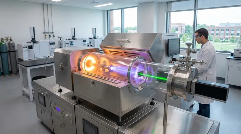
Chemical Vapor Deposition is a process where a solid thin film is grown on a substrate from gaseous molecules, known as precursors. This process is performed in a vacuum chamber.
For the film to form, the stable precursor gases must be broken apart into more reactive species. This requires an external input of energy, known as activation energy. The method used to supply this energy defines the specific type of CVD process.
The Primary Energy Sources in CVD
Each energy source creates the conditions for deposition in a fundamentally different way.
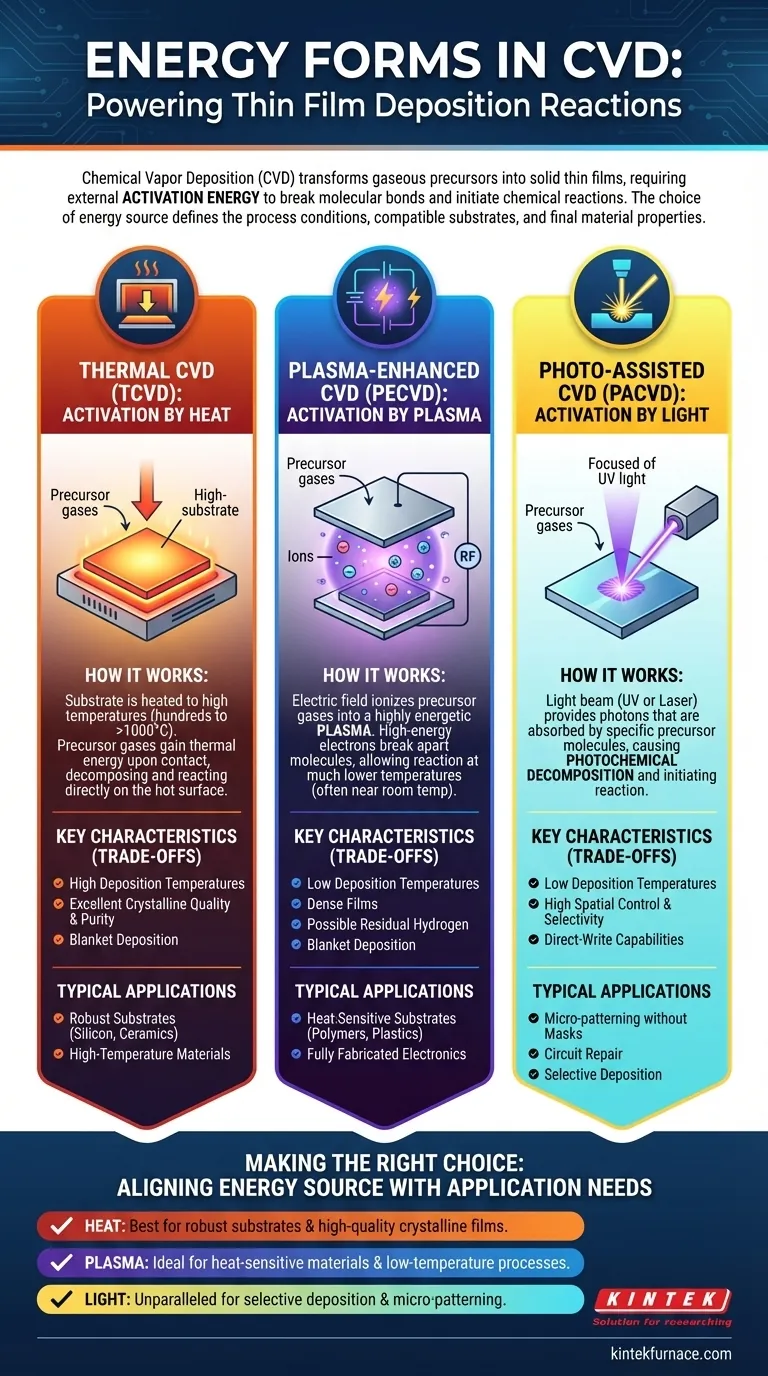
Thermal CVD (TCVD): Activation by Heat
In thermal CVD, the substrate itself is heated to a high temperature, often several hundred to over a thousand degrees Celsius.
When precursor gases flow over the hot substrate, they gain thermal energy, causing them to decompose and react directly on the surface. This is the most traditional and widely understood form of CVD.
Plasma-Enhanced CVD (PECVD): Activation by Plasma
PECVD uses an electric field to ionize the precursor gases, creating a plasma. A plasma is a highly energetic state of matter containing ions, electrons, and neutral particles.
The high-energy electrons within the plasma collide with and break apart the precursor gas molecules. This allows deposition to occur at much lower temperatures than in TCVD, often near room temperature.
Photo-Assisted CVD (PACVD): Activation by Light
This method uses a beam of light, typically from an ultraviolet (UV) lamp or a laser, to initiate the chemical reaction.
The precursor molecules are chosen specifically to absorb photons at the light source's wavelength. This absorption provides the energy to break their chemical bonds, a process known as photochemical decomposition.
Understanding the Trade-offs: Why the Energy Source Matters
The choice of activation method has direct consequences for the process window, compatible materials, and final film quality.
Impact on Process Temperature
The most significant trade-off is temperature. TCVD requires very high temperatures, which limits its use to substrates that can withstand extreme heat, like silicon wafers or ceramics.
PECVD and PACVD are considered "low-temperature" processes. This makes them essential for depositing films on temperature-sensitive substrates like plastics, polymers, or fully fabricated electronic devices.
Impact on Film Quality
High-temperature TCVD often produces films with high purity and excellent crystalline quality due to the thermal energy available for atoms to arrange themselves.
PECVD films, while deposited at lower temperatures, can sometimes have residual hydrogen (from precursors) or higher internal stress. However, the plasma bombardment can also create very dense films.
Impact on Control and Selectivity
TCVD and PECVD are typically "blanket" deposition techniques, meaning they coat every exposed surface inside the chamber.
Photo-assisted CVD, especially when using a focused laser (Laser-CVD), offers unique capabilities for direct-write processing. It allows for the selective deposition of material in a specific pattern without the need for masks.
Making the Right Choice for Your Application
The optimal energy source depends entirely on your material constraints and desired outcome.
- If your primary focus is depositing on robust, temperature-stable substrates: Thermal CVD is often the most direct and cost-effective method for high-quality films.
- If your primary focus is coating heat-sensitive materials like polymers or electronics: Plasma-enhanced CVD is the industry standard for low-temperature deposition.
- If your primary focus is creating specific micro-patterns or repairing circuits: Photo-assisted CVD provides unparalleled spatial control for selective deposition.
Ultimately, understanding these activation methods empowers you to select the precise CVD process that aligns with your technical and material requirements.
Summary Table:
| Energy Source | Key Characteristics | Typical Applications |
|---|---|---|
| Thermal (Heat) | High temperature (hundreds to over 1000°C), high purity and crystalline films | Robust substrates like silicon wafers and ceramics |
| Plasma (Electrical) | Low temperature (near room temperature), dense films, residual hydrogen possible | Heat-sensitive materials like polymers and electronics |
| Light (Radiant) | Low temperature, selective deposition with spatial control | Micro-patterning, circuit repair, direct-write processing |
Ready to optimize your CVD process with the right energy source? At KINTEK, we leverage exceptional R&D and in-house manufacturing to provide advanced high-temperature furnace solutions tailored to your needs. Our product line, including Muffle, Tube, Rotary Furnaces, Vacuum & Atmosphere Furnaces, and CVD/PECVD Systems, is complemented by strong deep customization capabilities to precisely meet your unique experimental requirements. Whether you're working with robust or heat-sensitive substrates, our expertise ensures superior film quality and process efficiency. Contact us today to discuss how we can enhance your laboratory's performance!
Visual Guide
Related Products
- Custom Made Versatile CVD Tube Furnace Chemical Vapor Deposition CVD Equipment Machine
- Split Chamber CVD Tube Furnace with Vacuum Station CVD Machine
- Multi Heating Zones CVD Tube Furnace Machine for Chemical Vapor Deposition Equipment
- Slide PECVD Tube Furnace with Liquid Gasifier PECVD Machine
- Controlled Inert Nitrogen Hydrogen Atmosphere Furnace
People Also Ask
- What future trends are expected in the development of CVD tube furnaces? Discover Smarter, More Versatile Systems
- What are the key features of CVD tube furnaces for 2D material processing? Unlock Precision Synthesis for Superior Materials
- What are the benefits of developing new precursor materials for CVD tube furnaces? Unlock Advanced Thin-Film Synthesis
- How can integrating CVD tube furnaces with other technologies benefit device fabrication? Unlock Advanced Hybrid Processes
- What are the practical applications of gate media prepared by CVD tube furnaces? Unlock Advanced Electronics and More


