At its core, a Chemical Vapor Deposition (CVD) furnace is a specialized system for building high-performance, solid materials one atomic layer at a time. Its primary applications are found in industries that rely on ultra-thin, highly pure films with specific properties. This includes manufacturing semiconductor chips, creating durable protective coatings for tools and implants, producing components for solar cells and LEDs, and synthesizing advanced materials like graphene.
The true value of a CVD furnace is not just its ability to apply a coating, but its precise control over the fundamental chemistry of material creation. This enables the fabrication of films with exceptional purity, uniformity, and performance that are often impossible to achieve through conventional methods.

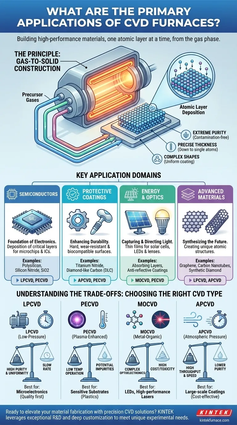
The Principle: Building Solid Materials from Gas
To understand the applications, you must first understand the process. A CVD furnace doesn't melt and cast material; it builds it chemically from a gaseous state.
How CVD Works: An Atomic Construction Process
Precursor gases, which contain the atoms of the desired material, are introduced into a high-temperature furnace chamber containing a substrate (the object to be coated). The heat triggers a chemical reaction, causing the atoms to "deposit" out of the gas and form a solid, thin film on the substrate's surface.
Think of it like frost forming on a cold window pane. Water vapor (the gas) hits the cold surface (the substrate) and condenses into a solid layer of ice (the film). CVD is a far more controlled version of this, using specific chemistry and high temperatures to build a perfect crystalline or amorphous layer.
Why This Method is So Powerful
This gas-to-solid approach gives CVD furnaces several key advantages. They can produce films with extreme purity, create layers with precise thickness control down to the single-atom level, and uniformly coat complex, three-dimensional shapes. This level of control is what makes CVD indispensable.
Key Application Domains Breakdown
The versatility of CVD allows it to be a cornerstone technology in several distinct, high-value industries.
The Semiconductor Industry: The Foundation of Electronics
This is the most well-known application. Modern microchips contain billions of transistors, each built from meticulously stacked layers of conductive, insulating, and semiconducting films.
CVD is used to deposit critical materials like polysilicon, silicon nitride, and silicon dioxide. The process's high purity and ability to create perfectly uniform films across an entire silicon wafer are essential for producing reliable integrated circuits.
Advanced Protective Coatings: Enhancing Durability
A microscopically thin CVD layer can fundamentally change the surface properties of a bulk material, making it dramatically more resistant to wear, corrosion, or heat.
Applications include depositing titanium nitride or diamond-like carbon onto cutting tools and drill bits to increase their hardness and lifespan. It is also used for creating biocompatible, wear-resistant coatings on medical implants like artificial hips and knees.
Energy & Optics: Capturing and Directing Light
CVD is critical for fabricating devices that interact with light. This involves depositing layers with specific optical or electrical properties.
It is used to create the thin-film absorbing layers in certain types of solar cells and to build up the complex, multi-layered structures of high-brightness LEDs. CVD is also used to apply anti-reflective coatings on lenses and mirrors.
Next-Generation Materials: Synthesizing the Future
Some of the most exciting new materials owe their existence to CVD. The unique properties of materials like graphene, carbon nanotubes, and synthetic diamond films are a direct result of their perfect atomic structure.
CVD is one of the few scalable methods capable of synthesizing these materials with the high quality required for applications in advanced electronics, composites, and thermal management.
Understanding the Trade-offs: Matching the Process to the Goal
Not all CVD processes are the same. The specific type of CVD furnace used is chosen based on a trade-off between deposition temperature, film quality, and cost.
Low-Pressure CVD (LPCVD): For Purity and Uniformity
Operating at a reduced pressure, LPCVD is the workhorse of the semiconductor industry. It produces exceptionally pure and uniform films over large areas, which is critical for wafer fabrication. The main trade-off is a relatively slow deposition rate.
Plasma-Enhanced CVD (PECVD): For Temperature-Sensitive Materials
PECVD uses plasma to energize the precursor gases, allowing the deposition reaction to occur at much lower temperatures. This is essential for coating substrates that cannot withstand high heat, such as plastics or fully assembled electronic devices. The trade-off is a potential for lower film quality or incorporated impurities from the plasma.
Metal-Organic CVD (MOCVD): For Complex Optoelectronics
This highly specialized technique uses metal-organic precursors to deposit complex compound semiconductor films. It is the go-to process for manufacturing high-performance lasers and multi-color LEDs. Its primary trade-offs are the high cost and toxicity of the precursor materials.
Atmospheric Pressure CVD (APCVD): For High Throughput
As the simplest variant, APCVD operates at normal atmospheric pressure, enabling fast deposition rates and high throughput. It is often used for lower-cost applications where perfect uniformity is less critical, such as applying protective coatings to architectural glass. The trade-off is generally lower film purity and quality.
Making the Right Choice for Your Application
Your goal determines the right technology. The choice is a balance of required performance, material constraints, and economic viability.
- If your primary focus is maximum film purity and uniformity for microelectronics: LPCVD is the industry standard for achieving the necessary quality.
- If your primary focus is depositing a film on a heat-sensitive substrate like a polymer: PECVD is the only viable option due to its low-temperature operation.
- If your primary focus is creating high-performance optoelectronic devices like LEDs: MOCVD provides the specialized capability required for these complex materials.
- If your primary focus is high-volume, low-cost coating: APCVD offers the best balance of speed and cost for less demanding applications.
Ultimately, selecting the right CVD process is about aligning the atomic-level deposition technique with the specific performance demands of your final product.
Summary Table:
| Application Domain | Key Uses | CVD Type Examples |
|---|---|---|
| Semiconductors | Depositing polysilicon, silicon nitride for microchips | LPCVD, PECVD |
| Protective Coatings | Hardening tools, biocompatible implants | APCVD, PECVD |
| Energy & Optics | Solar cells, LEDs, anti-reflective coatings | MOCVD, PECVD |
| Advanced Materials | Synthesizing graphene, carbon nanotubes | LPCVD, APCVD |
Ready to elevate your material fabrication with precision CVD solutions? At KINTEK, we leverage exceptional R&D and in-house manufacturing to provide advanced high-temperature furnace systems, including CVD/PECVD Systems, tailored for industries like semiconductors, energy, and medical devices. Our strong deep customization capability ensures we meet your unique experimental needs with high-purity, uniform films. Contact us today to discuss how our expertise can drive your innovations forward!
Visual Guide
Related Products
- Custom Made Versatile CVD Tube Furnace Chemical Vapor Deposition CVD Equipment Machine
- Split Chamber CVD Tube Furnace with Vacuum Station CVD Machine
- Multi Heating Zones CVD Tube Furnace Machine for Chemical Vapor Deposition Equipment
- Slide PECVD Tube Furnace with Liquid Gasifier PECVD Machine
- Inclined Rotary Plasma Enhanced Chemical Deposition PECVD Tube Furnace Machine
People Also Ask
- What is the working principle of a CVD tube furnace? Achieve Precise Thin Film Deposition for Your Lab
- What customization options are available for CVD tube furnaces? Tailor Your System for Superior Material Synthesis
- What are the practical applications of gate media prepared by CVD tube furnaces? Unlock Advanced Electronics and More
- What is a CVD tube furnace and what is its primary function? Discover Precision Thin-Film Deposition
- How does CVD tube furnace sintering enhance graphene growth? Achieve Superior Crystallinity and High Electron Mobility


