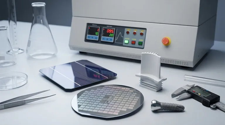
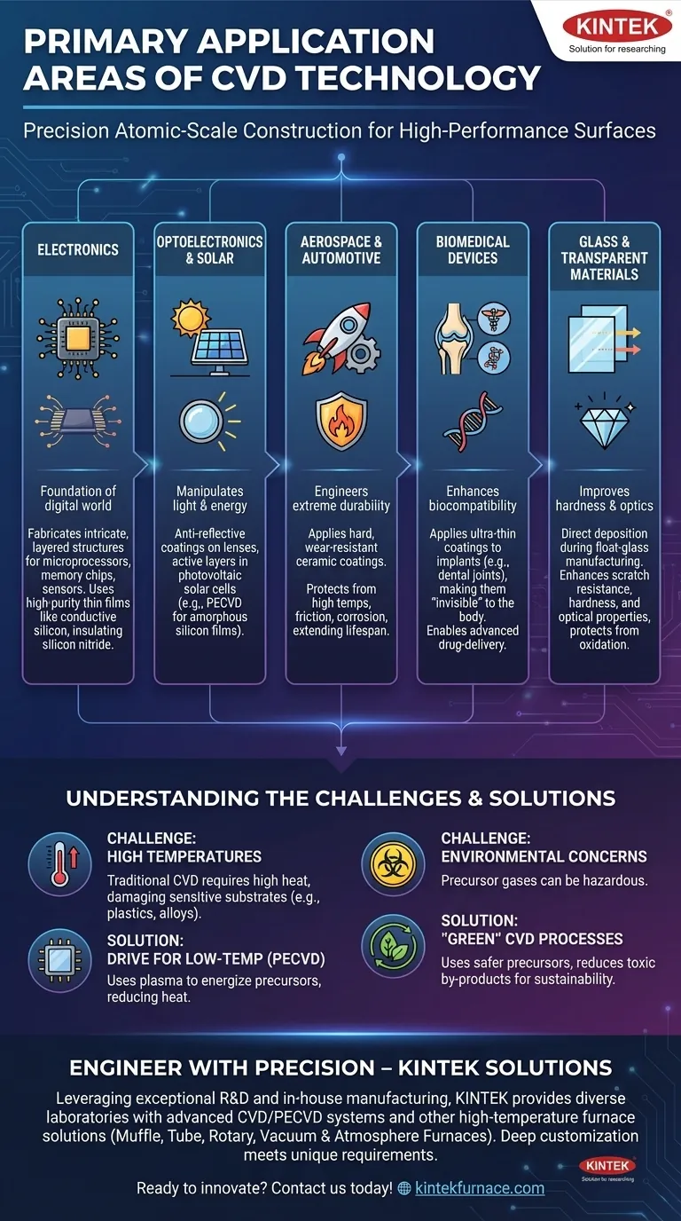
At its core, Chemical Vapor Deposition (CVD) is a foundational technology used to apply ultra-thin, high-performance films onto surfaces. Its primary applications are in semiconductor manufacturing for creating microchips, in optoelectronics for solar cells and optical coatings, and in surface engineering to create durable, protective layers for the aerospace, biomedical, and glass industries. CVD's value lies in its precision, allowing for the construction of materials atom by atom.
The true significance of CVD is not just the industries it serves, but its fundamental capability: it allows us to engineer the properties of a material's surface. By depositing a thin, highly controlled film, we can make-a-surface harder, more corrosion-resistant, biocompatible, or electrically conductive.
How CVD Enables Modern Technology
CVD is not a single tool but a versatile platform for atomic-scale construction. It works by introducing precursor gases into a chamber, which then react and deposit a solid, high-purity thin film onto a substrate material.
The Foundation of Electronics
The entire digital world is built on thin films. CVD is the indispensable process for fabricating the intricate, layered structures of integrated circuits.
Without it, modern microprocessors, memory chips, and sensors would be impossible to manufacture. It is used to deposit everything from conductive silicon films to insulating layers like silicon nitride.
Powering Optoelectronics and Solar Energy
CVD is critical for manipulating light and energy. It is used to apply anti-reflective coatings on lenses and to deposit the active layers in photovoltaic solar cells.
Specific variants like Plasma-Enhanced CVD (PECVD) are especially suited for creating the amorphous silicon films that are central to many thin-film solar devices.
Engineering Extreme Durability
In industries like aerospace and automotive, components must withstand extreme conditions. CVD is used to apply very hard, wear-resistant coatings, such as ceramic films.
These coatings protect critical parts from high temperatures, friction, and corrosion, dramatically extending their lifespan and reliability.
Advancing Biomedical Devices
The human body is quick to reject foreign materials. CVD is used to apply biocompatible coatings to medical implants, such as artificial joints and dental implants.
These ultra-thin layers make the implant "invisible" to the body's immune system, improving integration and patient outcomes. It is also explored for creating advanced drug-delivery systems.
Enhancing Glass and Transparent Materials
During the float-glass manufacturing process, CVD can be used to deposit a thin layer of silicon or other materials directly onto the hot glass surface.
This single step can dramatically improve the glass's hardness, scratch resistance, and optical properties, all while protecting it from oxidation.
Understanding the Practical Challenges
While incredibly powerful, CVD is not without its limitations. The process parameters have a direct impact on the quality of the final film and the integrity of the substrate.
The Problem of High Temperatures
Traditional CVD processes require very high temperatures to trigger the necessary chemical reactions. This heat can damage or deform the very part you are trying to coat.
This is a significant problem for temperature-sensitive substrates, such as plastics or certain metal alloys, limiting the application of some CVD methods.
The Drive for Low-Temperature Solutions
Much of the innovation in CVD technology is focused on lowering deposition temperatures. Techniques like PECVD use a plasma to energize the precursor gases, reducing the need for extreme heat.
This allows for the deposition of high-quality films on a wider range of materials without causing structural damage.
Environmental and Safety Concerns
The precursor gases used in CVD can be toxic, flammable, or corrosive, requiring sophisticated safety and handling protocols.
A major trend in the field is the development of "green" CVD processes that use less hazardous precursors and reduce toxic by-products, making the technology safer and more sustainable.
Applying This to Your Goal
The future of CVD is focused on greater control, efficiency, and sustainability, with AI-driven optimization and the production of novel 2D materials like graphene. How you leverage it depends entirely on your industry's core requirements.
- If your primary focus is electronics and manufacturing: CVD is the non-negotiable standard for creating the pure, uniform thin films required for microchips and sensors.
- If your primary focus is materials science and aerospace: CVD is your tool for engineering surfaces with extreme durability, heat resistance, and corrosion protection.
- If your primary focus is biomedical or renewable energy: CVD enables the creation of biocompatible surfaces and the efficient active layers needed for next-generation solar cells.
Ultimately, CVD is less a single application and more a fundamental platform technology that builds the high-performance surfaces of our modern world.
Summary Table:
| Application Area | Key Uses | Benefits |
|---|---|---|
| Electronics | Microchips, sensors, memory devices | High-purity films, precise layering |
| Optoelectronics | Solar cells, optical coatings | Enhanced light manipulation, energy efficiency |
| Aerospace & Automotive | Wear-resistant coatings | Extreme durability, corrosion protection |
| Biomedical | Implants, drug-delivery systems | Biocompatibility, improved patient outcomes |
| Glass & Transparent Materials | Hard coatings, scratch resistance | Increased hardness, optical enhancement |
Ready to engineer high-performance surfaces with precision? Leveraging exceptional R&D and in-house manufacturing, KINTEK provides diverse laboratories with advanced CVD/PECVD systems and other high-temperature furnace solutions like Muffle, Tube, Rotary, and Vacuum & Atmosphere Furnaces. Our strong deep customization capability ensures we precisely meet your unique experimental requirements, whether in electronics, aerospace, biomedical, or renewable energy. Contact us today to discuss how our tailored solutions can enhance your projects and drive innovation!
Visual Guide
Related Products
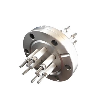
- Custom Made Versatile CVD Tube Furnace Chemical Vapor Deposition CVD Equipment Machine
- Multi Heating Zones CVD Tube Furnace Machine for Chemical Vapor Deposition Equipment
- HFCVD Machine System Equipment for Drawing Die Nano Diamond Coating
- Split Chamber CVD Tube Furnace with Vacuum Station CVD Machine
- 915MHz MPCVD Diamond Machine Microwave Plasma Chemical Vapor Deposition System Reactor
People Also Ask
- What is the working principle of a CVD tube furnace? Achieve Precise Thin Film Deposition for Your Lab
- How does CVD tube furnace sintering enhance graphene growth? Achieve Superior Crystallinity and High Electron Mobility
- What are the key application fields of CVD tube furnaces? Unlock Precision in Thin-Film Synthesis
- Why are CVD tube furnace sintering systems indispensable for 2D material research and production? Unlock Atomic-Scale Precision
- What is a CVD tube furnace and what is its primary function? Discover Precision Thin-Film Deposition