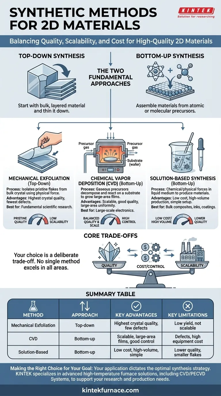
The creation of high-quality two-dimensional (2D) materials is driven by three primary synthesis methods: mechanical exfoliation, chemical vapor deposition (CVD), and solution-based synthesis. Mechanical exfoliation isolates pristine flakes from a bulk crystal, CVD grows large-area films from gaseous precursors, and solution-based methods produce material within a liquid medium. Each technique offers a distinct balance of material quality, scalability, and cost.
The central challenge in 2D material synthesis is not finding one "best" method, but rather selecting the right tool for the job. Your choice will always be a deliberate trade-off between crystalline perfection, production scale, and economic feasibility.
Top-Down vs. Bottom-Up: The Two Fundamental Approaches
The methods for creating 2D materials fall into two major categories. Top-down methods start with a bulk, layered material and thin it down, while bottom-up methods assemble materials from atomic or molecular precursors.
Top-Down Synthesis: Mechanical Exfoliation
Mechanical exfoliation is the classic "top-down" technique, famously used to first isolate graphene with adhesive tape. You begin with a bulk layered crystal and physically cleave or peel off layers until you are left with a single or few-layer sheet.
This method produces the highest-quality crystals with the fewest defects and impurities. The resulting flakes are nearly perfect, making them the gold standard for fundamental scientific research.
However, the process has extremely low yield and is not scalable. Flake size, shape, and location are random, making it unsuitable for any form of mass production.
Bottom-Up Synthesis: Building from Atoms
"Bottom-up" methods construct 2D materials by precisely adding atoms or molecules onto a surface. This approach offers far greater control over the final material's size and uniformity.
Chemical Vapor Deposition (CVD)
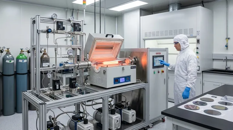
CVD is the most prominent bottom-up technique for high-quality, large-area 2D materials. In this process, precursor gases are introduced into a high-temperature furnace, where they decompose and react on the surface of a substrate (like copper or silicon) to form a continuous, uniform 2D film.
The primary advantage of CVD is its scalability. It is the leading method for producing wafer-scale films required for electronic and optoelectronic applications.
While quality is high, CVD-grown films can contain defects, such as grain boundaries, where different crystalline domains meet. The process also requires complex equipment, high temperatures, and vacuum conditions.
Solution-Based Synthesis
This broad category includes methods like liquid-phase exfoliation and hydrothermal synthesis. These techniques use chemical or physical forces within a liquid to either break down bulk crystals or precipitate 2D materials from dissolved precursors.
The main benefit is low cost and high-volume production. These methods are simple to implement and can generate large quantities of 2D material dispersed in a solvent, ideal for creating inks, composites, or coatings.
The trade-off is often lower material quality. Solution-synthesized flakes are typically smaller and may have more structural defects or chemical residues from surfactants, which can degrade electronic performance.
Understanding the Core Trade-offs
Choosing a synthesis method requires a clear understanding of its inherent compromises. No single method excels in all areas.
Quality vs. Scalability
This is the most critical trade-off. Mechanical exfoliation offers pristine quality but virtually zero scalability. On the other end, solution-based methods provide immense scalability but with compromised crystalline quality.
CVD sits in the middle, offering a powerful balance of good crystal quality and large-area industrial scalability, which is why it is so crucial for the electronics industry.
Cost vs. Control
Solution synthesis is by far the cheapest and simplest method, but it offers the least control over the final material's structure and purity.
CVD provides exceptional control over thickness and uniformity but requires a significant investment in complex, expensive equipment.
Application Fitness
The "best" method is defined by the end-use. Pristine flakes from exfoliation are essential for measuring intrinsic material properties in a lab. The minor defects in CVD films are often acceptable for large-area electronics. The lower quality of solution-processed material is perfectly suitable for applications where bulk properties, like conductivity in a composite, are more important than single-crystal perfection.
Making the Right Choice for Your Goal
Your application dictates the optimal synthesis strategy. Use these guidelines to make an informed decision.
- If your primary focus is fundamental research: Mechanical exfoliation is your best choice for obtaining pristine, defect-free samples for property measurement.
- If your primary focus is large-scale electronics: Chemical Vapor Deposition (CVD) is the industry standard for producing the uniform, wafer-scale films necessary for device fabrication.
- If your primary focus is bulk production for composites or inks: Solution-based synthesis offers the most cost-effective and scalable path to high-volume manufacturing.
Understanding these fundamental trade-offs empowers you to select the synthesis route that directly aligns with your project's technical and commercial objectives.
Summary Table:
| Method | Approach | Key Advantages | Key Limitations | Best For |
|---|---|---|---|---|
| Mechanical Exfoliation | Top-down | Highest crystal quality, few defects | Low yield, not scalable, random flake size | Fundamental research |
| Chemical Vapor Deposition (CVD) | Bottom-up | Scalable, large-area films, good control | Defects like grain boundaries, high equipment cost | Large-scale electronics |
| Solution-Based Synthesis | Bottom-up | Low cost, high-volume production, simple setup | Lower quality, smaller flakes, chemical residues | Bulk composites or inks |
Struggling to select the right synthesis method for your 2D materials? KINTEK specializes in advanced high-temperature furnace solutions, including CVD/PECVD Systems, to support your research and production needs. Leveraging our exceptional R&D and in-house manufacturing, we offer deep customization to precisely meet your unique experimental requirements. Whether you're developing large-area electronics or need scalable production tools, our expertise ensures optimal performance and efficiency. Contact us today to discuss how we can enhance your 2D material synthesis process!
Visual Guide
Related Products
- Custom Made Versatile CVD Tube Furnace Chemical Vapor Deposition CVD Equipment Machine
- Split Chamber CVD Tube Furnace with Vacuum Station CVD Machine
- Multi Heating Zones CVD Tube Furnace Machine for Chemical Vapor Deposition Equipment
- Slide PECVD Tube Furnace with Liquid Gasifier PECVD Machine
- Controlled Inert Nitrogen Hydrogen Atmosphere Furnace
People Also Ask
- What are the key application fields of CVD tube furnaces? Unlock Precision in Thin-Film Synthesis
- Why are CVD tube furnace sintering systems indispensable for 2D material research and production? Unlock Atomic-Scale Precision
- Which industries and research fields benefit from CVD tube furnace sintering systems for 2D materials? Unlock Next-Gen Tech Innovations
- What future trends are expected in the development of CVD tube furnaces? Discover Smarter, More Versatile Systems
- What temperature range do standard CVD tube furnaces operate at? Unlock Precision for Your Material Deposition


