The primary advantage of PECVD is its ability to deposit high-quality, dense thin films at significantly lower temperatures than traditional Chemical Vapor Deposition (CVD). This is achieved by using an energized plasma to drive the chemical reactions needed for deposition, rather than relying solely on high thermal energy. This fundamental difference makes PECVD ideal for applications involving heat-sensitive substrates and enables superior control over the final film's properties.
PECVD's core value is not just its lower temperature, but the control it provides. By replacing brute-force heat with targeted plasma energy, it decouples reaction rate from temperature, giving engineers and scientists precise command over the characteristics of the deposited material.
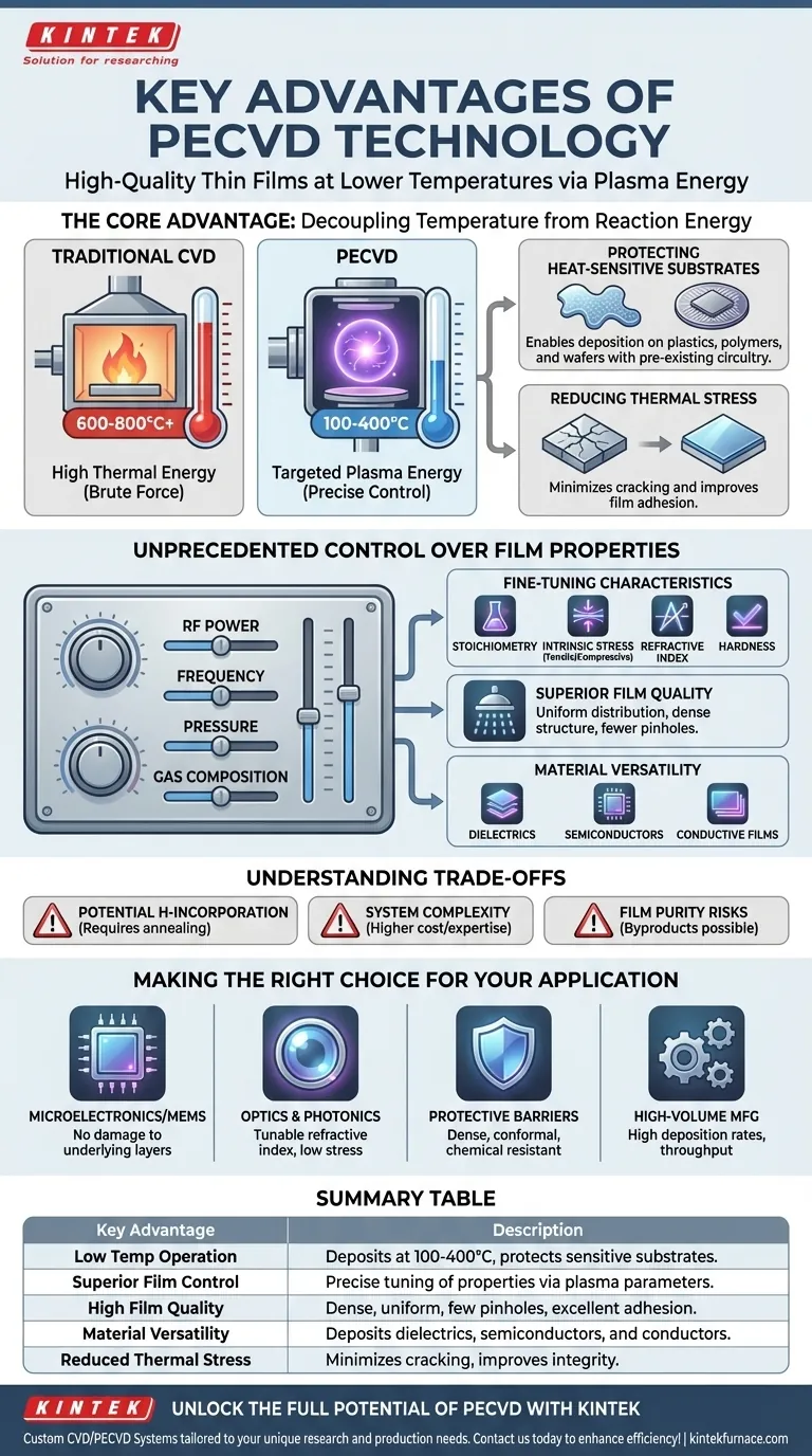
The Core Advantage: Decoupling Temperature from Reaction Energy
The defining feature of Plasma-Enhanced Chemical Vapor Deposition (PECVD) is the use of plasma—an ionized gas—to provide the energy for film formation. This fundamentally changes the deposition process compared to conventional thermal CVD.
Protecting Heat-Sensitive Substrates
In traditional CVD, temperatures of 600-800°C or higher are common. These temperatures would destroy or damage many materials.
PECVD operates at much lower temperatures, typically in the 100-400°C range. This makes it possible to deposit high-quality films on substrates like plastics, polymers, or semiconductor wafers with pre-existing metallic circuitry that cannot tolerate high heat.
Reducing Thermal Stress and Defects
High temperatures induce thermal stress as materials with different expansion coefficients cool down. This often leads to film cracking and poor adhesion.
By minimizing the process temperature, PECVD significantly reduces this thermal stress, resulting in films that are less prone to cracking and demonstrate excellent adhesion to the substrate.
Unprecedented Control Over Film Properties
The use of plasma provides multiple levers for tuning the deposition process. Adjusting parameters like RF power, frequency, pressure, and gas composition allows for precise engineering of the film's final characteristics.
Fine-Tuning Material Characteristics
Engineers can meticulously control the stoichiometry (the elemental ratio) of the film. For example, in silicon nitride (SiNx) deposition, the silicon-to-nitrogen ratio can be adjusted.
Advanced techniques, such as mixing high and low RF frequencies, allow for direct control over the intrinsic stress of the film, changing it from tensile to compressive to meet specific device requirements. Properties like refractive index and hardness can also be precisely tuned.
Achieving Superior Film Quality
PECVD systems often use a "showerhead" design for gas injection, which ensures a uniform distribution of precursor gases over the substrate. This results in films with excellent thickness uniformity.
The plasma-driven process creates highly reactive chemical species, leading to a very dense, cross-linked film structure with fewer pinholes compared to other methods. This density is critical for creating effective barrier layers.
Expanding Material Versatility
PECVD is an extremely versatile technique capable of depositing a wide range of materials. This includes dielectrics (silicon dioxide, silicon nitride), semiconductors (amorphous silicon), and even some conductive films.
Understanding the Trade-offs
While powerful, PECVD is not a universal solution. Understanding its limitations is key to making an informed decision.
Potential for Hydrogen Incorporation
Many PECVD processes use precursor gases containing hydrogen (like silane, SiH₄). The plasma can cause hydrogen atoms to be incorporated into the growing film.
This incorporated hydrogen can sometimes negatively impact the film's electrical properties, a critical consideration for certain electronic and optoelectronic devices. Post-deposition annealing is often required to drive it out.
System Complexity
PECVD systems are more complex than simple thermal CVD furnaces. They require RF power generators, impedance matching networks, and sophisticated vacuum controls to maintain and manage the plasma.
This complexity can translate to higher initial equipment costs and a need for more specialized process engineering expertise.
Film Purity and Byproducts
Because the process is chemical, there is always a risk of precursor byproducts being incorporated into the film, affecting its ultimate purity.
For applications requiring the absolute highest purity, a physical method like Physical Vapor Deposition (PVD) might be preferable, as it does not involve chemical reactions.
Making the Right Choice for Your Application
Selecting the right deposition technology depends entirely on your end goal and material constraints.
- If your primary focus is microelectronics or MEMS: Choose PECVD for its ability to deposit high-quality dielectrics without damaging underlying metal layers or sensitive components.
- If your primary focus is optics or photonics: Leverage PECVD for its precise, tunable control over refractive index and low-stress films, which are critical for waveguides and anti-reflection coatings.
- If your primary focus is creating protective barriers: Use PECVD to produce dense, pinhole-free, and highly conformal coatings that provide excellent corrosion and chemical resistance.
- If your primary focus is high-volume manufacturing: Capitalize on PECVD's high deposition rates, which offer significant throughput advantages over conventional CVD and many PVD techniques.
By understanding how plasma fundamentally alters the deposition process, you can effectively leverage PECVD to achieve material properties that are otherwise unattainable.
Summary Table:
| Key Advantage | Description |
|---|---|
| Low Temperature Operation | Deposits films at 100-400°C, protecting heat-sensitive substrates like plastics and semiconductors. |
| Superior Film Control | Allows precise tuning of stoichiometry, stress, refractive index, and hardness via plasma parameters. |
| High Film Quality | Produces dense, uniform films with excellent adhesion and fewer pinholes for effective barriers. |
| Material Versatility | Capable of depositing dielectrics, semiconductors, and conductive films for various uses. |
| Reduced Thermal Stress | Minimizes cracking and improves film integrity by lowering process temperatures. |
Unlock the full potential of PECVD for your laboratory! At KINTEK, we leverage exceptional R&D and in-house manufacturing to provide advanced high-temperature furnace solutions, including our specialized CVD/PECVD Systems. Our strong deep customization capability ensures we can precisely meet your unique experimental requirements, whether you're working with microelectronics, optics, protective barriers, or high-volume manufacturing. Contact us today to discuss how our tailored PECVD solutions can enhance your research and production efficiency!
Visual Guide
Related Products
- RF PECVD System Radio Frequency Plasma Enhanced Chemical Vapor Deposition
- Slide PECVD Tube Furnace with Liquid Gasifier PECVD Machine
- Inclined Rotary Plasma Enhanced Chemical Deposition PECVD Tube Furnace Machine
- Inclined Rotary Plasma Enhanced Chemical Deposition PECVD Tube Furnace Machine
- Cylindrical Resonator MPCVD Machine System for Lab Diamond Growth
People Also Ask
- What is the role of RF power in PECVD and how does the RF-PECVD process work? Master Thin Film Deposition Control
- What is PECVD specification? A Guide to Choosing the Right System for Your Lab
- How are deposition rates and film properties controlled in PECVD? Master Key Parameters for Optimal Thin Films
- What are the applications of plasma enhanced chemical vapor deposition? Key Uses in Electronics, Optics & Materials
- What is RF in PECVD? A Critical Control for Plasma Deposition


