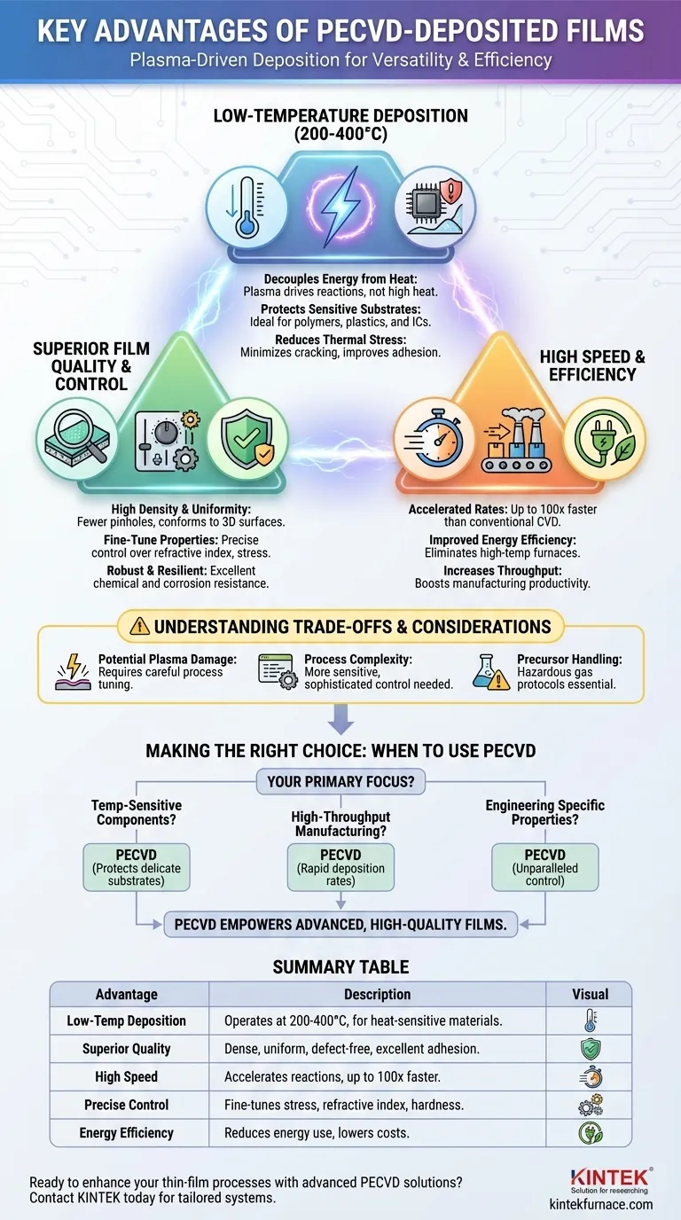
The primary advantages of PECVD-deposited films are their ability to be formed at low temperatures, their superior quality and uniformity, and the high speed at which they can be deposited. This combination makes Plasma-Enhanced Chemical Vapor Deposition (PECVD) a uniquely versatile and efficient technology for creating protective, optical, and electronic thin films on a wide variety of materials.
At its core, the power of PECVD comes from using an energy-rich plasma to drive chemical reactions instead of high heat. This fundamental difference decouples the deposition process from the substrate's thermal limits, enabling the creation of high-quality films in situations where traditional methods would fail.
The Core Advantage: Plasma-Driven Deposition at Low Temperatures
The most significant benefit of PECVD is its ability to operate at much lower temperatures (typically 200-400°C) than conventional Chemical Vapor Deposition (CVD), which often requires temperatures above 600°C.
Decoupling Energy from Heat
In traditional CVD, high temperatures are necessary to provide the thermal energy needed to break down precursor gases and initiate the chemical reactions that form the film.
PECVD replaces this thermal energy with energy from a plasma. The plasma creates highly reactive ions and radicals that can react and deposit at much lower temperatures.
Protecting Temperature-Sensitive Substrates
This low-temperature process is critical for depositing films on materials that cannot withstand high heat. This includes polymers, plastics, and fully fabricated semiconductor devices with sensitive integrated circuits.
Reducing Thermal Stress and Cracking
By minimizing the temperature difference between the deposition process and the final operating environment, PECVD significantly reduces the thermal stress within the film. This results in films that are much less prone to cracking and have better adhesion to the substrate.
Superior Film Quality and Control
The plasma environment not only lowers the temperature but also provides a unique level of control over the film's final properties, leading to superior performance.
Achieving High Density and Uniformity
PECVD produces films that are highly uniform across the entire substrate, even on complex, three-dimensional surfaces. The resulting layers are dense and highly cross-linked, leading to fewer pinholes and defects compared to other methods.
Fine-Tuning Material Properties
Process engineers can precisely manipulate the final film by adjusting plasma parameters like power, pressure, and gas composition. This allows for exceptional control over critical material properties such as refractive index, film stress, hardness, and chemical stoichiometry.
Building Robust, Resilient Films
The dense, highly cross-linked structure of PECVD films provides outstanding resistance to chemical attack, solvents, and corrosion. This makes it an ideal process for creating durable protective coatings and encapsulation layers.
Optimizing for Speed and Efficiency
For industrial applications, throughput and cost are major factors. PECVD offers significant advantages in both areas.
Accelerating Deposition Rates
The highly reactive species generated in the plasma accelerate the chemical reactions, leading to very high deposition rates. For some materials, like silicon nitride, PECVD can be over 100 times faster than conventional CVD, dramatically increasing manufacturing throughput.
Improving Energy Efficiency
By eliminating the need for high-temperature furnaces, PECVD systems can be more energy-efficient. This not only reduces operational costs but also contributes to a cleaner manufacturing process.
Understanding the Trade-offs and Considerations
While powerful, PECVD is not a universal solution. Its advantages come with complexities that must be managed for successful implementation.
Potential for Plasma Damage
The high-energy ions within the plasma can sometimes cause damage to the surface of a sensitive substrate. This requires careful tuning of the process to balance deposition rate against potential damage.
Process and Equipment Complexity
PECVD systems are more complex and often more expensive than some alternative deposition techniques like thermal evaporation or sputtering. The process itself is highly sensitive to parameters, demanding sophisticated control and process development.
Precursor Chemical Handling
Like all CVD processes, PECVD relies on precursor gases that can be hazardous, flammable, or corrosive. This necessitates robust safety protocols and gas handling infrastructure.
Making the Right Choice for Your Application
Selecting a deposition method depends entirely on your project's primary constraints and desired outcomes.
- If your primary focus is processing temperature-sensitive components: PECVD is an outstanding choice, as its low-temperature nature protects delicate substrates like plastics or integrated circuits.
- If your primary focus is high-throughput manufacturing: The rapid deposition rates of PECVD offer a clear advantage for scaling production and reducing cycle times.
- If your primary focus is engineering specific film properties: PECVD provides an unparalleled level of control over characteristics like stress and refractive index, making it ideal for advanced optical and electronic applications.
Ultimately, PECVD empowers you to create advanced, high-quality films on materials and with properties that are simply unattainable with high-temperature methods.
Summary Table:
| Advantage | Description |
|---|---|
| Low-Temperature Deposition | Operates at 200-400°C, ideal for heat-sensitive substrates like plastics and semiconductors. |
| Superior Film Quality | Produces dense, uniform, and defect-free films with excellent adhesion and chemical resistance. |
| High Deposition Speed | Accelerates reactions for faster throughput, up to 100x quicker than conventional CVD in some cases. |
| Precise Property Control | Allows fine-tuning of stress, refractive index, and hardness via plasma parameters. |
| Energy Efficiency | Reduces energy use by eliminating high-temperature heating, lowering operational costs. |
Ready to enhance your thin-film processes with advanced PECVD solutions? At KINTEK, we leverage exceptional R&D and in-house manufacturing to provide diverse laboratories with cutting-edge high-temperature furnace solutions, including our specialized CVD/PECVD Systems. Our strong deep customization capability ensures we precisely meet your unique experimental requirements, whether for electronics, optics, or protective coatings. Contact us today to discuss how our tailored PECVD systems can drive efficiency and innovation in your applications!
Visual Guide
Related Products
- Slide PECVD Tube Furnace with Liquid Gasifier PECVD Machine
- RF PECVD System Radio Frequency Plasma Enhanced Chemical Vapor Deposition
- Inclined Rotary Plasma Enhanced Chemical Deposition PECVD Tube Furnace Machine
- Inclined Rotary Plasma Enhanced Chemical Deposition PECVD Tube Furnace Machine
- Multi Heating Zones CVD Tube Furnace Machine for Chemical Vapor Deposition Equipment
People Also Ask
- What is plasma in the context of PECVD? Unlock Low-Temperature Thin Film Deposition
- In which industries is the tube furnace commonly used? Essential for Materials Science, Energy, and More
- How does PECVD equipment contribute to TOPCon bottom cells? Mastering Hydrogenation for Maximum Solar Efficiency
- What plasma source is used in PE-CVD tube furnaces? Unlock Low-Temperature, High-Quality Deposition
- How does a hydrogen reduction environment in an industrial tube furnace facilitate gold-copper alloy microspheres?


