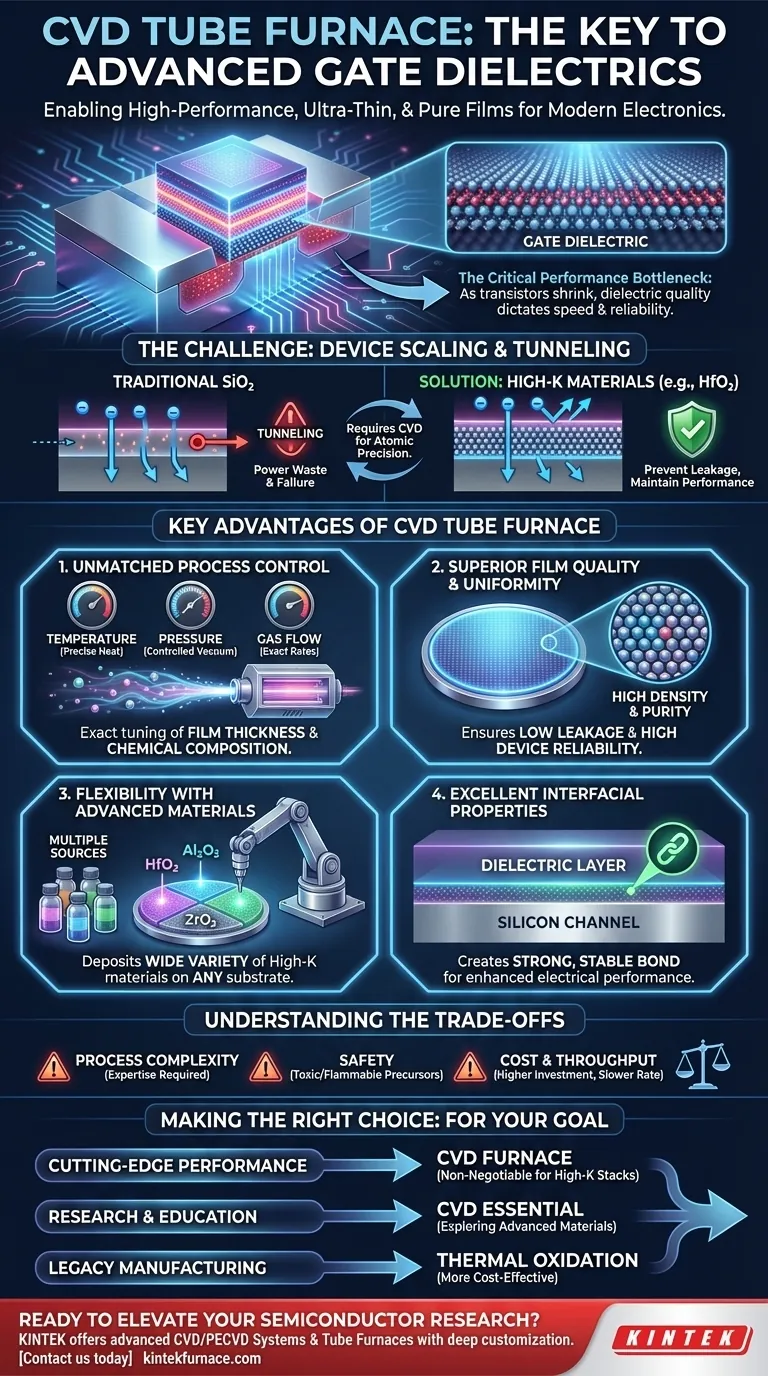
In short, a Chemical Vapor Deposition (CVD) tube furnace is the preferred tool for preparing modern gate dielectrics because it enables the deposition of exceptionally high-quality, uniform, and pure thin films. This method provides the precise control over temperature, gas flow, and pressure necessary to create the advanced, ultra-thin high-K materials that are essential for the performance and reliability of state-of-the-art transistors.
As transistors shrink to the atomic scale, the gate dielectric becomes a critical performance bottleneck. A CVD tube furnace directly solves this by allowing engineers to move beyond traditional materials and precisely construct advanced dielectric layers فيلم by film, a capability essential for modern electronics.
Why Precise Control is Non-Negotiable
To understand the furnace's advantages, you must first appreciate the gate dielectric's role. It is the heart of a transistor, a thin insulating layer that controls the flow of electrical current.
The Gate Dielectric's Critical Role
The quality of this single, ultra-thin layer dictates the transistor's speed, power consumption, and reliability. Any imperfection, impurity, or variation in thickness can lead to current leakage or device failure.
The Challenge of Device Scaling
For decades, silicon dioxide (SiO2) was the standard gate dielectric. However, as transistors shrank, this layer had to become so thin (only a few atoms thick) that electrons began to "tunnel" through it, causing massive power waste.
The solution was to use new high-K materials (like hafnium oxide, HfO2), which can be physically thicker to prevent leakage while providing the same electrical performance. These materials cannot be simply "grown" on silicon; they must be deposited with atomic-level precision. This is where CVD becomes indispensable.
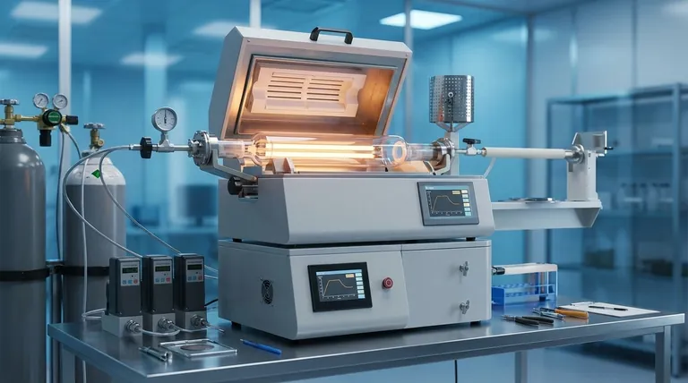
Key Advantages of the CVD Tube Furnace
The CVD tube furnace provides the controlled environment necessary to execute this delicate deposition process, offering a combination of control, quality, and material flexibility that other methods cannot match.
Unmatched Process Control
A CVD furnace allows for the independent and precise manipulation of all critical process parameters. This includes temperature, pressure, and the flow rate of precursor gases.
This level of control allows for the exact tuning of the film's final properties, most importantly its thickness and chemical composition.
Superior Film Quality and Uniformity
The stable, sealed environment декорации a tube furnace ensures that the deposited films are of the highest quality. This results in films that are exceptionally uniform across the entire wafer, highly dense with minimal defects, and extremely pure.
High purity is critical, as it prevents unwanted chemical reactions and ensures the film has the desired insulating properties, leading to lower leakage current and higher device reliability.
Flexibility with Advanced Materials
Unlike thermal oxidation, which is limited to growing oxides of the underlying substrate (like SiO2 on silicon), CVD is a deposition process.
This means you can deposit a wide variety of materials onto any suitable substrate. This flexibility is the key reason CVD is used for high-K dielectrics, as it allows for the deposition of materials like HfO2, Al2O3, and others that are central to modern semiconductor technology.
Excellent Interfacial Properties
The bond between the gate dielectric and the silicon channel beneath it is critical. A poor interface leads to a slow and unreliable transistor.
CVD processes can be optimized to create a clean, sharp, and stable interface. This ensures a strong bonding force and excellent electrical characteristics, directly enhancing device stability and performance.
Understanding the Trade-offs
While powerful, the CVD tube furnace is not a universally simple solution. Its advantages come with inherent complexities.
Process Complexity
CVD relies on complex chemical reactions from volatile precursor gases. Developing a stable and repeatable process recipe requires significant expertise and experimentation.
Precursor Handling and Safety
The precursor chemicals used in CVD are often toxic, flammable, or pyrophoric. Using a CVD furnace requires stringent safety protocols, specialized gas handling cabinets, and robust emergency-response systems.
Cost and Throughput
CVD systems, especially those designed for high-purity semiconductor work, are significantly more expensive and complex than simple thermal oxidation furnaces. The deposition process can also be slower, impacting manufacturing throughput.
Making the Right Choice for Your Goal
The decision to use a CVD tube furnace depends entirely on the requirements of the gate dielectric you intend to create.
- If your primary focus is cutting-edge device performance: The precise control and material flexibility of a CVD furnace are non-negotiable for fabricating high-performance gate stacks with modern high-K dielectrics.
- If your primary focus is fundamental research or education: While thermal oxidation is simpler for demonstrating basic SiO2 capacitors, a CVD system is essential for exploring any non-silicon-based or advanced dielectric materials.
- If your primary focus is high-volume, legacy node manufacturing: For thicker, less demanding dielectrics on older process nodes, simpler and higher-throughput methods like thermal oxidation may remain more cost-effective.
Ultimately, the CVD tube furnace is the enabling technology fatores the creation of the advanced gate dielectrics that are fundamental to modern, high-performance electronics.
Summary Table:
| Advantage | Description |
|---|---|
| Precise Control | Independent manipulation of temperature, pressure, and gas flow for exact film properties. |
| Superior Film Quality | Ensures uniform, dense, and pure films with minimal defects. |
| Material Flexibility | Deposits various high-K materials like HfO2 and Al2O3 on different substrates. |
| Excellent Interfacial Properties | Creates clean, sharp interfaces for stable bonding and enhanced electrical performance. |
Ready to elevate your semiconductor research with advanced high-temperature furnace solutions? KINTEK, leveraging exceptional R&D and in-house manufacturing, offers a diverse product line including CVD/PECVD Systems, Tube Furnaces, and more, with strong deep customization to precisely meet your unique experimental needs. Contact us today to discuss how our solutions can enhance your gate dielectric preparation and boost device performance!
Visual Guide
Related Products
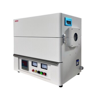
- Custom Made Versatile CVD Tube Furnace Chemical Vapor Deposition CVD Equipment Machine
- Split Chamber CVD Tube Furnace with Vacuum Station CVD Machine
- Multi Heating Zones CVD Tube Furnace Machine for Chemical Vapor Deposition Equipment
- Slide PECVD Tube Furnace with Liquid Gasifier PECVD Machine
- Inclined Rotary Plasma Enhanced Chemical Deposition PECVD Tube Furnace Machine
People Also Ask
- What are the benefits of developing new precursor materials for CVD tube furnaces? Unlock Advanced Thin-Film Synthesis
- What improvements can be made to the bonding force of gate dielectric films using a CVD tube furnace? Enhance Adhesion for Reliable Devices
- How might AI and machine learning enhance CVD tube furnace processes? Boost Quality, Speed, and Safety
- What customization options are available for CVD tube furnaces? Tailor Your System for Superior Material Synthesis
- How does CVD tube furnace sintering enhance graphene growth? Achieve Superior Crystallinity and High Electron Mobility