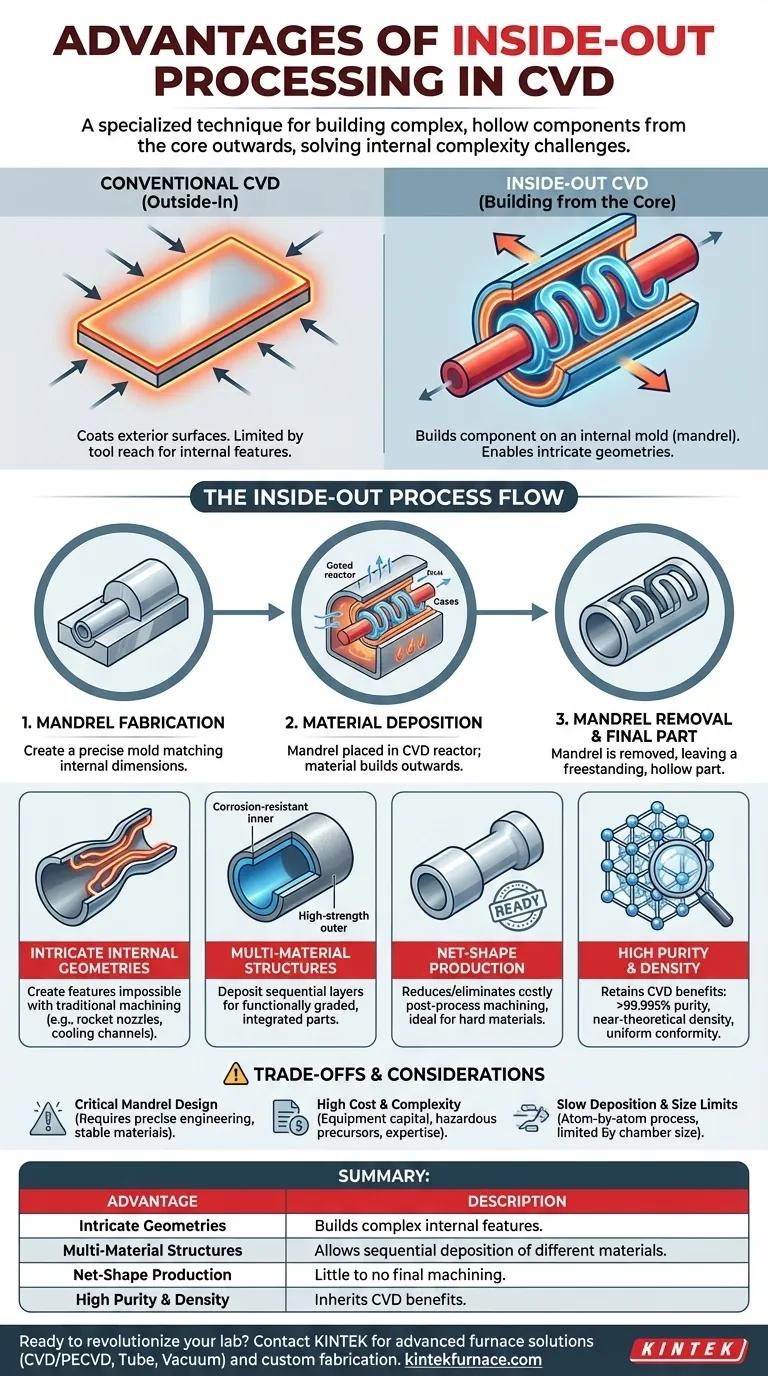
Inside-out Chemical Vapor Deposition (CVD) is a specialized fabrication technique that fundamentally changes how complex, hollow components are created. Unlike conventional methods that build or machine parts from the outside in, this process builds the component on an internal mold. Its primary advantages are the ability to fabricate intricate internal geometries, create multi-material composite structures, and produce net-shape parts that require little to no final machining.
The core challenge in advanced manufacturing is often not the external shape of a component, but its internal complexity. Inside-out CVD solves this by building the part from the inside out on a removable form (a mandrel), enabling the creation of integrated, high-performance designs that are impossible to make with traditional methods.
Understanding the Inside-Out Process
To appreciate its advantages, it's crucial to distinguish inside-out CVD from the conventional approach. The difference lies in where the material deposition occurs.
The Conventional CVD Method
In a standard CVD process, gaseous precursors react on the heated surface of a substrate, depositing a thin film or coating. This is an "outside-in" process, excellent for coating the exterior surfaces of an existing component.
The Inside-Out Method: Building from the Core
Inside-out CVD flips this concept. The process involves three key steps:
- Mandrel Fabrication: A precision form, or mandrel, is created that matches the exact internal dimensions of the desired component.
- Deposition: The mandrel is placed in a CVD reactor, and the desired material (or materials) is deposited onto its surface. The part is literally built from its inner wall outwards.
- Mandrel Removal: After deposition is complete, the mandrel is removed, typically by chemical etching or melting, leaving behind a freestanding, hollow component.
Key Advantages of the Inside-Out Approach
This unique manufacturing sequence unlocks capabilities that are difficult or impossible to achieve otherwise.
Unlocking Intricate Internal Geometries
The primary advantage is the ability to create complex internal features. The complexity is no longer limited by the reach of a cutting tool but by the ability to fabricate the mandrel, which is often much simpler.
This is critical for components like rocket engine nozzles, advanced heat exchangers, or cooling channels that require optimized, non-linear passages for fluid or gas flow.
Fabricating Multi-Material and Lined Structures
The inside-out process is ideal for creating functionally graded materials. By changing the precursor gases during deposition, you can build up sequential layers of different materials.
This allows for the creation of a single, integrated component with, for example, a highly corrosion-resistant inner layer and a high-strength structural outer layer, without any joints or welds.
Achieving Net-Shape Production
Because the deposition process forms the final component directly, it yields net-shape or near-net-shape parts. This drastically reduces or eliminates the need for costly and time-consuming post-process machining.
This benefit is especially significant when working with very hard or difficult-to-machine materials, such as ceramics or refractory metals.
Inheriting the Core Strengths of CVD
Finally, the inside-out method retains all the fundamental benefits of the CVD process itself, including the ability to produce materials with extremely high purity (>99.995%), near-theoretical density, and excellent, uniform conformity.
Understanding the Trade-offs and Limitations
While powerful, inside-out CVD is a specialized technique with its own set of challenges that make it unsuitable for every application.
The Mandrel is a Critical Constraint
The success of the entire process hinges on the mandrel. It must be precisely fabricated, stable enough to withstand the high temperatures of the CVD process, and, most importantly, easily and completely removable without damaging the final part. The engineering of the mandrel is often a significant project in itself.
Process Costs and Complexity
Like most CVD processes, the equipment has a high capital cost. The precursor gases can be expensive and are often hazardous, requiring specialized handling protocols and safety systems. Controlling the process parameters to achieve the desired material properties requires significant expertise.
Deposition Time and Component Size
CVD is an atom-by-atom or molecule-by-molecule deposition process, which can be slow. It is not well-suited for high-volume, low-cost manufacturing. The ultimate size of the component is also limited by the physical dimensions of the CVD reaction chamber.
When to Choose Inside-Out CVD
This technique should be considered a strategic solution for specific, high-value engineering challenges.
- If your primary focus is producing components with complex internal channels: Inside-out CVD is a leading solution, as the internal geometry is defined by the more easily fabricated mandrel rather than a machine tool's path.
- If your primary focus is creating integrated, multi-material parts: This method allows you to deposit distinct layers of different materials in a single, seamless process to optimize performance.
- If your primary focus is avoiding difficult post-process machining: Inside-out CVD produces net-shape parts with high precision, making it ideal for creating components from extremely hard or brittle materials.
By understanding its specific capabilities, you can leverage inside-out CVD to fabricate next-generation components that were previously considered impossible.
Summary Table:
| Advantage | Description |
|---|---|
| Intricate Internal Geometries | Builds complex internal features using a removable mandrel, enabling designs impossible with traditional methods. |
| Multi-Material Structures | Allows sequential deposition of different materials for functionally graded, seamless components. |
| Net-Shape Production | Produces parts that require little to no final machining, reducing costs and time. |
| High Purity and Density | Inherits CVD benefits for materials with >99.995% purity and uniform conformity. |
Ready to revolutionize your lab with advanced high-temperature furnace solutions? At KINTEK, we leverage exceptional R&D and in-house manufacturing to provide diverse laboratories with cutting-edge equipment like CVD/PECVD Systems, Muffle, Tube, Rotary Furnaces, and Vacuum & Atmosphere Furnaces. Our strong deep customization capability ensures we precisely meet your unique experimental requirements for complex component fabrication. Contact us today to discuss how our solutions can enhance your research and production efficiency!
Visual Guide
Related Products
- Split Chamber CVD Tube Furnace with Vacuum Station CVD Machine
- Multi Heating Zones CVD Tube Furnace Machine for Chemical Vapor Deposition Equipment
- HFCVD Machine System Equipment for Drawing Die Nano Diamond Coating
- Custom Made Versatile CVD Tube Furnace Chemical Vapor Deposition CVD Equipment Machine
- Inclined Rotary Plasma Enhanced Chemical Deposition PECVD Tube Furnace Machine
People Also Ask
- How might AI and machine learning enhance CVD tube furnace processes? Boost Quality, Speed, and Safety
- What are the practical applications of gate media prepared by CVD tube furnaces? Unlock Advanced Electronics and More
- What temperature range do standard CVD tube furnaces operate at? Unlock Precision for Your Material Deposition
- What are the advantages of using a CVD tube furnace for preparing gate dielectrics? Achieve High-Quality Thin Films for Transistors
- How does a CVD tube furnace achieve high purity in gate media preparation? Master Precision Control for Flawless Films


