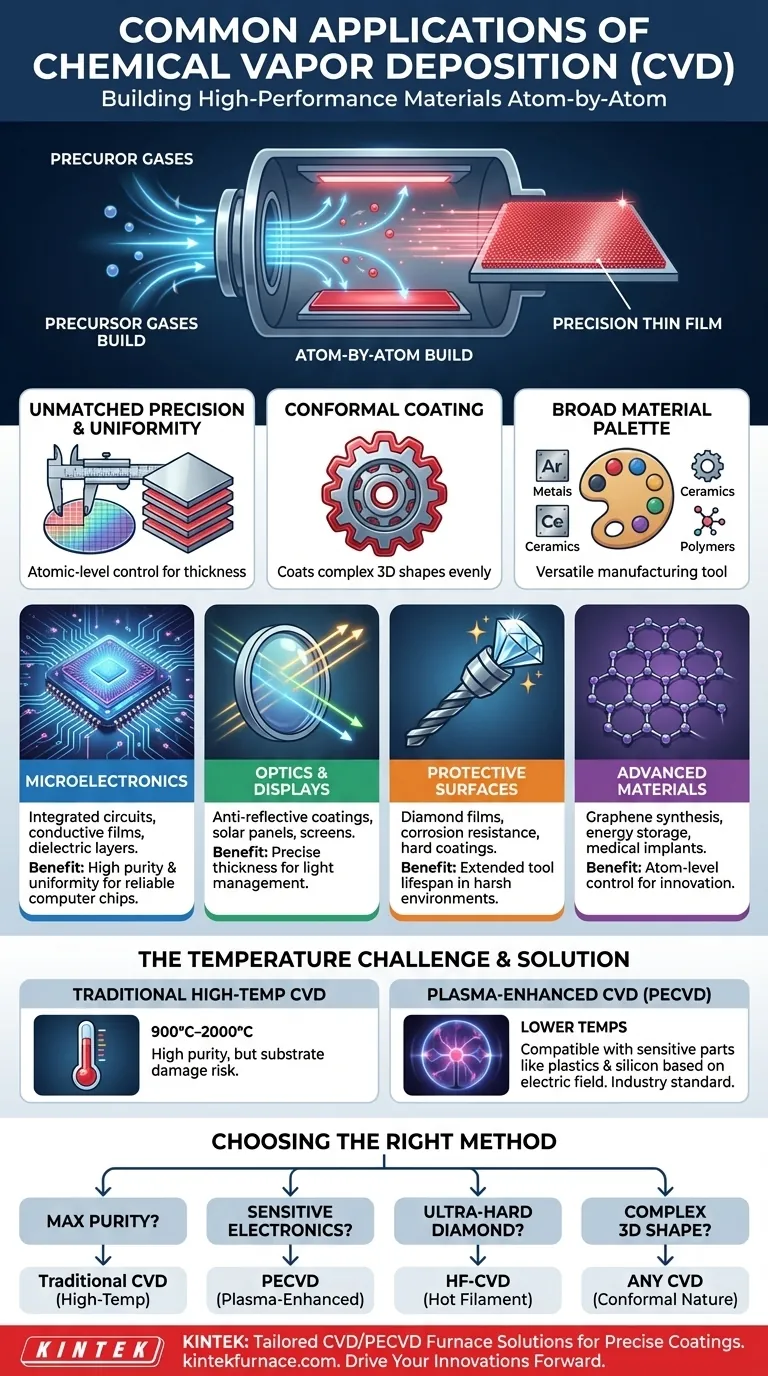
At its core, Chemical Vapor Deposition (CVD) is a foundational manufacturing process for creating high-performance thin films and coatings. Its most common applications are in the fabrication of microelectronics like computer chips, the creation of optical coatings for lenses and displays, and the production of advanced materials such as synthetic diamond and protective layers for industrial tools.
The true value of CVD lies not just in what it creates, but how. It is a family of processes that builds materials atom-by-atom from a gas, enabling unmatched control over purity, thickness, and uniformity on virtually any surface shape.
What Makes CVD So Versatile?
The power of CVD comes from a few fundamental principles that make it adaptable to an enormous range of industrial and scientific challenges.
The Core Principle: Building from the Atom Up
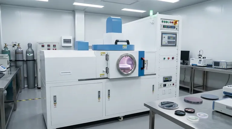
CVD is a process where a substrate (the part to be coated) is placed in a vacuum chamber and exposed to one or more volatile precursor gases.
When heated, these gases react or decompose, causing a solid material to deposit onto the substrate surface. Because it happens at a chemical level, the resulting film is exceptionally pure and well-bonded.
Unmatched Precision and Uniformity
The process allows for precise, atomic-level control over the thickness and composition of the deposited film.
This ability to create ultra-thin, perfectly uniform layers is essential for modern electronics, where the performance of a transistor can depend on a film just a few atoms thick.
Conformal Coating on Complex Shapes
Unlike "line-of-sight" processes like spray painting, the precursor gases in a CVD chamber flow around and coat all exposed surfaces of an object equally.
This conformal coating is critical for ensuring complete coverage on complex 3D parts, from intricate micro-mechanical devices (MEMS) to industrial machine components.
A Broad Material Palette
By changing the precursor gases and reaction conditions, CVD can be used to deposit a vast array of materials. This includes metals, ceramics, and even certain polymers, making it a highly flexible manufacturing tool.
A Closer Look at Key Applications
This versatility has made CVD an indispensable process in several high-tech industries.
In Microelectronics and Semiconductors
This is arguably the most significant application of CVD. It is used to deposit the critical layers that make up integrated circuits, including dielectric layers for insulation, conductive films for wiring, and the semiconductor materials themselves.
The high purity and uniformity of CVD films are non-negotiable for producing reliable, high-performance computer chips, memory, and processors.
In Optics and Displays
CVD is used to apply thin films for anti-reflective coatings on lenses and solar panels, mirrors, and optical filters.
The process's precise control over film thickness is used to tune how light interacts with a surface, enhancing transmission, reflection, or filtering specific wavelengths. This is also key in manufacturing flat-panel displays.
For Protective and High-Performance Surfaces
The technique is widely used to create extremely hard and durable coatings. Diamond films deposited via CVD are applied to cutting tools to dramatically increase their lifespan and performance.
It is also used to apply coatings that protect mechanical parts from high-temperature oxidation and corrosion, extending their operational life in harsh environments.
For Advanced and Future Materials
CVD is at the forefront of materials science. It is a primary method for synthesizing graphene, producing materials for energy storage devices, and creating biocompatible coatings for medical implants.
Understanding the Trade-offs: The Challenge of Temperature
While powerful, CVD is not a single, one-size-fits-all solution. The primary trade-off to manage is the operational temperature.
The Drawback of Traditional High-Temperature CVD
Traditional CVD processes require very high temperatures, often between 900°C and 2000°C, to trigger the necessary chemical reactions.
These extreme temperatures can damage or deform the substrate material, limiting the types of parts that can be coated. For example, you could not use high-temperature CVD on a plastic part or many sensitive electronic components.
The Solution: Plasma-Enhanced CVD (PECVD)
To overcome this limitation, variations like Plasma-Enhanced CVD (PECVD) were developed. PECVD uses an electric field to generate a plasma (an ionized gas), which provides the energy for the reaction.
This allows deposition to occur at much lower temperatures, making it compatible with temperature-sensitive substrates like silicon wafers, plastics, and glass used in solar cells and flat-panel displays. PECVD is the workhorse of the modern semiconductor industry for this reason.
Other Specialized CVD Methods
Other variations exist to solve specific problems. Hot Filament CVD (HF-CVD) is optimized for producing high-quality synthetic diamond films, while methods like Direct Liquid Injection CVD are suited for depositing complex metal oxides.
Making the Right Choice for Your Goal
Selecting the correct CVD variant depends entirely on the material you are depositing and the substrate you are coating.
- If your primary focus is maximum purity and crystallinity: Traditional, high-temperature CVD is often the best choice, provided your substrate can withstand the heat.
- If your primary focus is coating temperature-sensitive electronics or polymers: Plasma-Enhanced CVD (PECVD) is the industry standard and the most logical approach.
- If your primary focus is creating ultra-hard diamond coatings: A specialized process like Hot Filament CVD (HF-CVD) is specifically designed for that outcome.
- If your primary focus is achieving uniform coverage on a complex 3D part: The conformal nature of nearly all CVD processes makes them superior to line-of-sight deposition methods.
Ultimately, Chemical Vapor Deposition is a foundational engineering tool that enables the creation of materials that would be impossible to manufacture otherwise.
Summary Table:
| Application Area | Key Uses | CVD Benefits |
|---|---|---|
| Microelectronics | Integrated circuits, conductive films | High purity, uniform layers for reliability |
| Optics | Anti-reflective coatings, displays | Precise thickness control for light management |
| Protective Surfaces | Diamond coatings, corrosion resistance | Hard, durable films for extended tool life |
| Advanced Materials | Graphene synthesis, medical implants | Atom-level control for innovative materials |
Ready to enhance your lab's capabilities with tailored high-temperature furnace solutions? KINTEK leverages exceptional R&D and in-house manufacturing to provide advanced furnaces like Muffle, Tube, Rotary, Vacuum & Atmosphere, and CVD/PECVD Systems. Our deep customization ensures they meet your unique experimental needs for precise, uniform coatings. Contact us today to discuss how our solutions can drive your innovations forward!
Visual Guide
Related Products
- Custom Made Versatile CVD Tube Furnace Chemical Vapor Deposition CVD Equipment Machine
- RF PECVD System Radio Frequency Plasma Enhanced Chemical Vapor Deposition
- MPCVD Machine System Reactor Bell-jar Resonator for Lab and Diamond Growth
- 915MHz MPCVD Diamond Machine Microwave Plasma Chemical Vapor Deposition System Reactor
- Slide PECVD Tube Furnace with Liquid Gasifier PECVD Machine
People Also Ask
- How does CVD tube furnace sintering enhance graphene growth? Achieve Superior Crystallinity and High Electron Mobility
- What future trends are expected in the development of CVD tube furnaces? Discover Smarter, More Versatile Systems
- What is a CVD tube furnace and what is its primary function? Discover Precision Thin-Film Deposition
- What are the practical applications of gate media prepared by CVD tube furnaces? Unlock Advanced Electronics and More
- What are the benefits of developing new precursor materials for CVD tube furnaces? Unlock Advanced Thin-Film Synthesis


