To deposit silicon dioxide using PECVD, precursor gases containing silicon and oxygen are introduced into a vacuum chamber and energized into a plasma. This plasma creates highly reactive chemical species that deposit onto a substrate as a thin SiO₂ film. This method is distinct because the plasma energy, rather than high heat, drives the reaction, allowing for high-quality deposition at significantly lower temperatures.
The central challenge in depositing dielectric films is doing so without damaging the underlying electronic components. PECVD solves this by substituting thermal energy with plasma energy, enabling the growth of robust silicon dioxide films at temperatures low enough (< 400°C) to protect sensitive, fully-fabricated device structures.
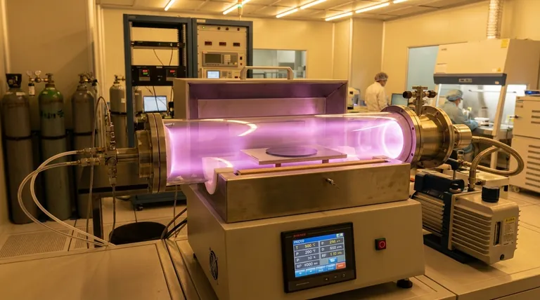
The PECVD Mechanism: From Gas to Solid Film
The PECVD process for silicon dioxide is a precisely controlled, multi-step sequence that transforms gases into a solid layer on a substrate, typically a silicon wafer.
Step 1: Introducing Precursor Gases
The process begins by feeding a controlled mixture of gases into a low-pressure reaction chamber. These gases must supply the necessary silicon and oxygen atoms.
Common silicon precursors include silane (SiH₄) gas or a vaporized liquid source like tetraethylorthosilicate (TEOS). Common oxygen precursors include oxygen (O₂) or nitrous oxide (N₂O).
Step 2: Generating the Plasma
A high-frequency radio frequency (RF) electric field is applied across the chamber. This energy strips electrons from the gas molecules, creating a glowing, ionized gas known as a plasma.
This plasma is a reactive soup of ions, radicals, and electrons. This "enhancement" is the key to PECVD, as these species are far more chemically reactive than the original stable gas molecules.
Step 3: Diffusion and Surface Reaction
The reactive species generated in the plasma diffuse and travel to the substrate surface. Because they are already in a high-energy, reactive state, they do not need high thermal energy from the substrate to react.
Once on the surface, they undergo chemical reactions to form stable silicon dioxide (SiO₂) molecules.
Step 4: Film Growth and By-product Removal
The SiO₂ molecules bond to the substrate, forming a thin, solid film. This film grows layer by layer as the process continues.
Volatile by-products from the reaction, such as hydrogen (H₂), are continuously removed from the chamber by the vacuum system.
Key Recipes and Their Characteristics
The choice of precursor gases directly impacts the properties of the final SiO₂ film and the conditions required for deposition.
The Silane-Based Process
Using silane (SiH₄) with nitrous oxide (N₂O) or **oxygen (O₂) ** is a common method. It works well at low temperatures, typically between 300-400°C.
However, films grown from silane often incorporate hydrogen, which can sometimes impact the film's electrical properties. Silane gas is also pyrophoric, meaning it can ignite on contact with air, requiring strict safety protocols.
The TEOS-Based Process
Using TEOS as the silicon source is an extremely common industry practice. As a liquid, TEOS is significantly safer to handle and store than silane.
TEOS-based PECVD typically produces films with better conformality—the ability to evenly coat complex, non-flat surfaces. This makes it ideal for depositing insulating layers between metal lines in an integrated circuit.
High-Density Plasma (HDP-CVD)
A more advanced variant, High-Density Plasma CVD, uses a higher-density plasma to achieve superior results. An HDP process using silane and oxygen can produce nearly hydrogen-free SiO₂ films with excellent gap-fill capabilities and good conformality.
Understanding the Trade-offs: Why Choose PECVD?
No deposition technique is perfect for every application. Choosing PECVD involves weighing its primary advantage against its inherent limitations.
The Primary Advantage: Low Temperature
The single most important reason to use PECVD is its low deposition temperature (< 400°C). Other methods like LPCVD (Low-Pressure CVD) often require temperatures of 650-900°C.
This low thermal budget is critical for "back-end-of-line" processing, where transistors and other structures are already present on the wafer. High temperatures would damage metallic components like aluminum interconnects.
Film Quality and Hydrogen Content
The primary trade-off is film quality. PECVD SiO₂ is generally less dense and has a higher concentration of embedded hydrogen compared to films grown at high temperatures (like thermal oxide or LPCVD oxide).
This lower density can result in slightly inferior electrical insulation properties. For applications demanding the highest possible purity and dielectric strength, a high-temperature method may be necessary if the device can tolerate it.
Deposition Rate vs. Conformality
PECVD offers a relatively high deposition rate, which is advantageous for manufacturing throughput. However, its conformality can be less perfect than that achieved with slower, higher-temperature LPCVD processes. As noted, using TEOS or HDP-CVD can significantly mitigate this limitation.
Making the Right Choice for Your Goal
Your choice of deposition method should be dictated by the specific requirements of your device and its stage of fabrication.
- If your primary focus is protecting temperature-sensitive underlying layers: PECVD is the definitive choice due to its low processing temperature.
- If your primary focus is achieving the highest possible film purity and density: High-temperature thermal oxidation or LPCVD are superior, provided your device can withstand the heat.
- If your primary focus is balancing safety, film quality, and good step coverage: A TEOS-based PECVD process is the preferred industry standard for interlayer dielectrics.
Understanding these fundamental trade-offs empowers you to select the precise deposition method that aligns with your specific device fabrication requirements.
Summary Table:
| Aspect | Details |
|---|---|
| Process | Uses plasma to energize precursor gases (e.g., SiH₄, TEOS, O₂, N₂O) for SiO₂ deposition |
| Temperature | Low temperature (<400°C), ideal for back-end-of-line processing |
| Key Advantages | Protects sensitive components, high deposition rates, good conformality with TEOS |
| Common Applications | Interlayer dielectrics in integrated circuits, coating non-flat surfaces |
| Trade-offs | Lower density and higher hydrogen content vs. high-temperature methods |
Optimize Your Silicon Dioxide Deposition with KINTEK's Advanced PECVD Solutions!
Are you working with temperature-sensitive electronics or need precise SiO₂ films for your lab? KINTEK leverages exceptional R&D and in-house manufacturing to provide high-temperature furnace solutions, including our specialized CVD/PECVD Systems. Our products, such as Muffle, Tube, Rotary Furnaces, Vacuum & Atmosphere Furnaces, and CVD/PECVD Systems, are designed for diverse laboratory needs. With strong deep customization capabilities, we tailor our solutions to meet your unique experimental requirements—ensuring high-quality, low-temperature deposition that protects your devices and boosts efficiency.
Contact us today to discuss how KINTEK can enhance your fabrication processes and deliver reliable results!
Visual Guide

Related Products
- Inclined Rotary Plasma Enhanced Chemical Deposition PECVD Tube Furnace Machine
- RF PECVD System Radio Frequency Plasma Enhanced Chemical Vapor Deposition
- Slide PECVD Tube Furnace with Liquid Gasifier PECVD Machine
- Inclined Rotary Plasma Enhanced Chemical Deposition PECVD Tube Furnace Machine
- Custom Made Versatile CVD Tube Furnace Chemical Vapor Deposition CVD Equipment Machine
People Also Ask
- What types of materials can be processed in rotary tube furnaces? Optimize Your Thermal Processing with Versatile Solutions
- What are the technical advantages of using a rotary tube furnace for hydrochar activation? Achieve Superior Porosity
- When are rotary tube furnaces not suitable for a process? Avoid Costly Mistakes in Thermal Processing
- What is plasma in the context of PECVD? Unlock Low-Temperature Thin Film Deposition
- What optional features enhance the processing capabilities of rotary tube furnaces? Boost Efficiency with Advanced Customizations


