When comparing film quality, the primary distinction is not that one method is universally superior, but that each excels under different conditions. Plasma-Enhanced Chemical Vapor Deposition (PECVD) generally produces higher quality films with better density and fewer defects on temperature-sensitive substrates. Conventional Chemical Vapor Deposition (CVD), while capable of producing high-quality films, is better suited for applications where high heat is acceptable and complex surface coverage is critical.
The core difference lies in the energy source. PECVD uses plasma to enable film deposition at low temperatures, minimizing thermal stress. Traditional CVD relies on high heat, which introduces trade-offs between deposition speed, conformality, and potential thermal damage to the substrate.
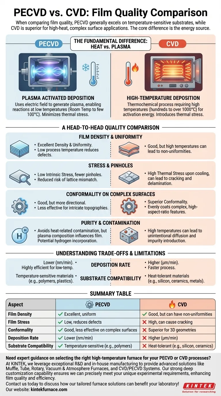
The Fundamental Difference: Heat vs. Plasma
To understand the quality differences, you must first understand how each process works. The energy source dictates the operating window and resulting film characteristics.
CVD: Deposition Driven by High Temperature
Conventional CVD is a thermochemical process. It requires high temperatures, often ranging from several hundred to over a thousand degrees Celsius.
This intense heat provides the necessary activation energy to break down precursor gases, allowing them to react and deposit as a solid film on the substrate surface.
PECVD: Deposition Activated by Plasma
PECVD operates on a different principle. It uses an electric field to generate plasma, an ionized gas containing high-energy electrons and ions.
These energetic particles transfer their energy to the precursor gases, enabling chemical reactions at much lower temperatures—from room temperature up to a few hundred degrees Celsius. This avoids the need for intense thermal energy.
A Head-to-Head Quality Comparison
The difference in energy source directly impacts the final film's structural and mechanical properties.
Film Density and Uniformity
PECVD often produces films with excellent density and uniformity. The lower process temperature reduces thermal stress, preventing defects and ensuring a more consistent layer.
While CVD can also produce uniform films, the high temperatures can sometimes lead to non-uniformities if thermal gradients exist across the substrate.
Stress and Pinholes
This is a key advantage for PECVD. By operating at low temperatures, it significantly reduces intrinsic film stress and the risk of lattice mismatch between the film and the substrate. This results in fewer pinholes and a more stable film.
High-temperature CVD inherently introduces thermal stress as the coated substrate cools, which can lead to cracking, delamination, or defect formation.
Conformality on Complex Surfaces
Conventional CVD typically offers superior conformality. The high thermal energy and gas-phase reactions allow the film to evenly coat complex, three-dimensional geometries and high-aspect-ratio features.
PECVD, while good, may exhibit more directionality, making it slightly less effective for coating extremely intricate topographies compared to thermal CVD.
Purity and Contamination
Purity can be a concern for both methods, but for different reasons. The high temperatures in CVD can sometimes lead to unintentional diffusion or reactions, potentially introducing impurities.
PECVD avoids heat-related contamination but introduces its own variable: the plasma itself. The composition of the plasma can influence the film's chemical makeup, and incomplete reactions can sometimes leave byproducts like hydrogen in the film.
Understanding the Trade-offs and Limitations
Choosing between CVD and PECVD requires weighing their respective advantages against your project's specific constraints.
Deposition Rate: The Speed Factor
Generally, traditional CVD offers a higher deposition rate, capable of depositing material from tens of nanometers to several micrometers per minute.
PECVD typically has a lower deposition rate, on the order of a few to tens of nanometers per minute. However, it is considered highly efficient for a low-temperature process.
Substrate Compatibility
This is often the deciding factor. The low operating temperature of PECVD makes it compatible with temperature-sensitive materials like polymers, plastics, and integrated circuits with existing layers.
The high heat of CVD restricts its use to substrates that can withstand extreme temperatures without damage or degradation, such as silicon wafers, ceramics, or metals.
Performance Limitations of PECVD
While versatile, PECVD films have known limitations. They can be softer and have weaker wear resistance compared to films deposited by other methods.
Additionally, their performance as a barrier coating (e.g., against moisture) can be less robust than specialized coatings and is highly dependent on the specific plasma chemistry and film thickness used.
Making the Right Choice for Your Application
Your decision should be guided by the primary requirements of your substrate and desired film properties.
- If your primary focus is coating a temperature-sensitive electronic device or polymer: PECVD is the definitive choice, as it prevents thermal damage while delivering a high-quality, low-stress film.
- If your primary focus is achieving a highly conformal coating on a complex, heat-tolerant 3D object: Traditional CVD is superior due to its excellent surface coverage capabilities.
- If your primary focus is maximizing deposition speed on a substrate that can handle high heat: High-temperature CVD is generally the faster process.
By understanding the fundamental trade-off between thermal energy and plasma activation, you can confidently select the deposition method that aligns with your specific engineering goals.
Summary Table:
| Aspect | PECVD | CVD |
|---|---|---|
| Film Density | Excellent, uniform | Good, but can have non-uniformities |
| Film Stress | Low, reduces defects | High, can cause cracking |
| Conformality | Good, less effective on complex surfaces | Superior for 3D geometries |
| Deposition Rate | Lower (nm/min) | Higher (μm/min) |
| Substrate Compatibility | Temperature-sensitive (e.g., polymers) | Heat-tolerant (e.g., silicon, ceramics) |
Need expert guidance on selecting the right high-temperature furnace for your PECVD or CVD processes? At KINTEK, we leverage exceptional R&D and in-house manufacturing to provide advanced solutions like Muffle, Tube, Rotary, Vacuum & Atmosphere Furnaces, and CVD/PECVD Systems. Our strong deep customization capability ensures we can precisely meet your unique experimental requirements, enhancing film quality and efficiency. Contact us today to discuss how our tailored furnace solutions can benefit your laboratory!
Visual Guide
Related Products
- RF PECVD System Radio Frequency Plasma Enhanced Chemical Vapor Deposition
- Slide PECVD Tube Furnace with Liquid Gasifier PECVD Machine
- Inclined Rotary Plasma Enhanced Chemical Deposition PECVD Tube Furnace Machine
- Inclined Rotary Plasma Enhanced Chemical Deposition PECVD Tube Furnace Machine
- Cylindrical Resonator MPCVD Machine System for Lab Diamond Growth
People Also Ask
- What are some promising applications of PECVD-prepared 2D materials? Unlock Advanced Sensing and Optoelectronics
- What is PECVD specification? A Guide to Choosing the Right System for Your Lab
- What are the advantages of PECVD in film deposition? Achieve Low-Temp, High-Quality Coatings
- How are deposition rates and film properties controlled in PECVD? Master Key Parameters for Optimal Thin Films
- What are the applications of plasma enhanced chemical vapor deposition? Key Uses in Electronics, Optics & Materials


