At its core, a vacuum annealing furnace is an indispensable tool in electronic material research because it allows scientists to heat materials in a highly controlled environment, free from atmospheric contamination. This process is used to test and refine a material's fundamental thermal, electrical, and mechanical properties, providing the critical data needed to develop next-generation electronic components.
The crucial function of a vacuum furnace is not just the heat it applies, but the air it removes. By eliminating reactive gases like oxygen, researchers can isolate the effects of thermal energy on a material's atomic structure, ensuring that observed changes are a direct result of the process, not a byproduct of unwanted chemical reactions.
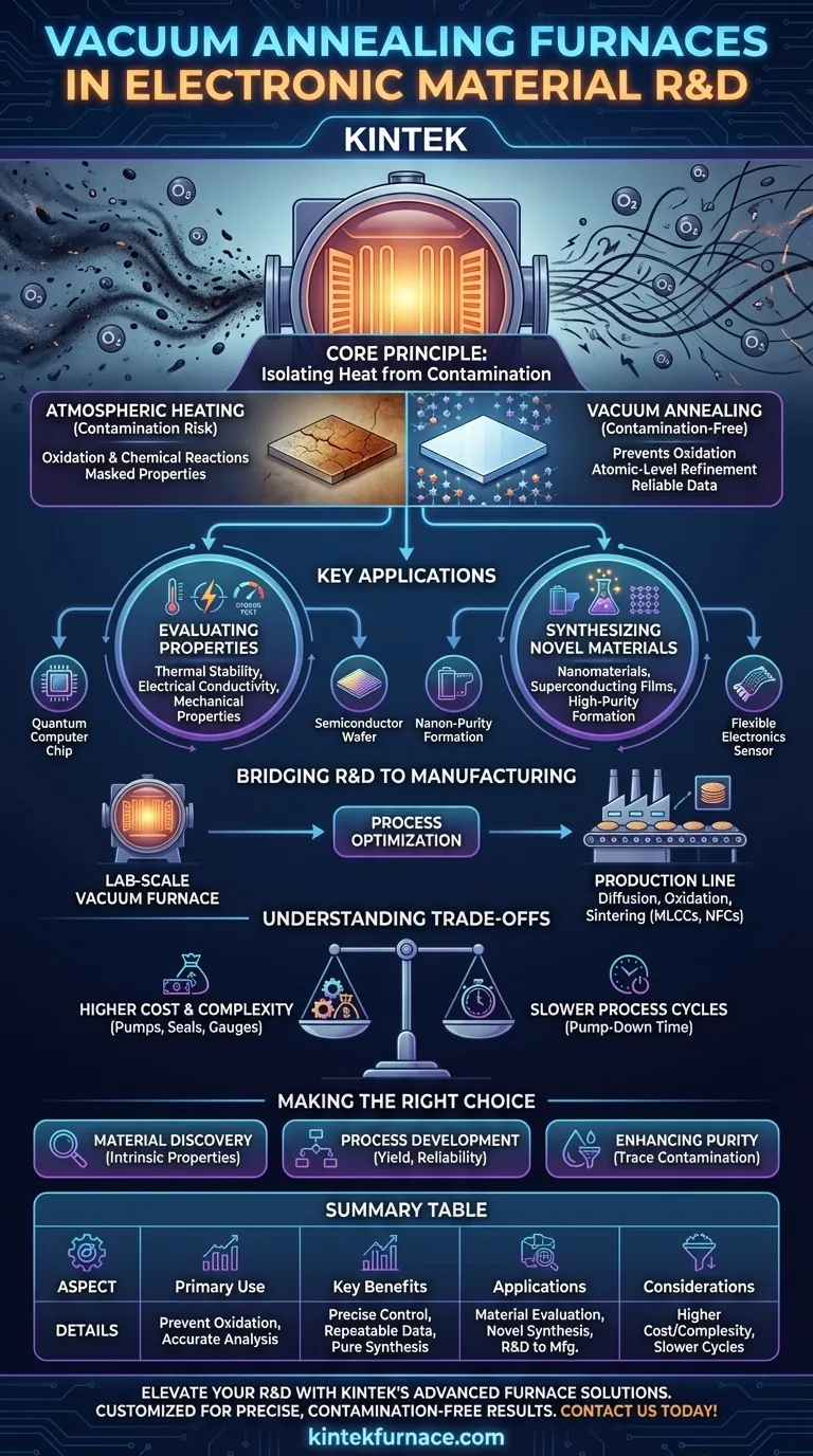
The Core Principle: Isolating Heat from Contamination
The primary purpose of using a vacuum for heat treatment is to create an environment that is as pure as possible. This is not a trivial detail; it is fundamental to obtaining meaningful results in material science.
Why a Vacuum is Non-Negotiable
When materials are heated in the presence of air, they can oxidize. This oxidation fundamentally alters the material's surface and bulk properties, masking the true effects of the annealing process.
A vacuum furnace removes these reactive gases, preventing oxidation and other forms of contamination. This ensures that any change in the material—such as improved conductivity or reduced internal stress—is a direct result of the controlled heating and cooling cycle.
Achieving Atomic-Level Refinement
Annealing is a process designed to alter a material's microstructure. It can relieve internal stresses, increase ductility, and refine the grain structure, which directly impacts electrical performance.
By performing this in a vacuum, researchers can be certain that these structural changes are driven purely by thermal energy rearranging the crystal lattice, not by chemical reactions with atmospheric gases. This precision is vital for developing materials with highly specific and predictable behaviors.
Ensuring Repeatable and Reliable Data
Scientific progress depends on the ability to repeat experiments and get consistent results. Vacuum furnaces provide a precisely controlled and replicable environment.
This allows researchers to systematically test how different annealing temperatures, ramp rates, and hold times affect a material, generating the reliable data needed to optimize it for a specific application.
Key Applications in Electronic Material R&D
In the lab, these furnaces are used for two primary functions: evaluating existing materials and synthesizing entirely new ones. The controlled environment is critical for both.
Evaluating Material Properties
Researchers use vacuum furnaces to subject new materials to simulated processing conditions. They can precisely measure how properties like thermal stability and electrical conductivity change after heat treatment.
This data is crucial for determining if a new alloy, semiconductor, or superconductor is suitable for its intended application, from a simple circuit to a complex quantum computer.
Synthesizing Novel Materials
For cutting-edge materials like nanomaterials and superconducting films, purity is paramount from the moment of creation. A vacuum furnace provides the ideal high-temperature, high-purity environment for material formation and growth.
This process ensures that these highly sensitive materials are not compromised by impurities, which could render them useless.
Bridging Research to Manufacturing
The insights gained in R&D directly inform large-scale manufacturing. Processes developed and tested in a lab-scale vacuum furnace are later applied to production lines.
This includes critical steps in making the electronics we use every day, such as semiconductor wafer diffusion and oxidation, as well as the sintering of ceramic components like MLCCs and NFCs.
Understanding the Trade-offs
While essential, vacuum furnaces are a specific tool with their own set of considerations. Understanding their limitations is key to using them effectively.
Higher Cost and Complexity
Vacuum systems, with their associated pumps, seals, and gauges, are inherently more complex and expensive to acquire and maintain than standard atmospheric furnaces.
Slower Process Cycles
Achieving a high vacuum requires a "pump-down" time before the heating cycle can even begin. This can make the overall process time longer compared to treatments in an ambient or inert gas environment.
When a Simpler Tool Suffices
For materials that are not sensitive to oxidation or for processes where some level of atmospheric interaction is acceptable or even desired, a simpler and less expensive inert gas or atmospheric furnace may be a more practical choice.
Making the Right Choice for Your Goal
The decision to use a vacuum annealing furnace should be driven by the specific requirements of your material and the objective of your research.
- If your primary focus is fundamental material discovery: The furnace is your tool for uncovering a material's intrinsic properties without the interference of environmental variables.
- If your primary focus is process development: Use the furnace to precisely simulate and optimize manufacturing steps to improve the yield, reliability, and performance of a final product.
- If your primary focus is enhancing material purity: The vacuum environment is non-negotiable for synthesizing or annealing materials where even trace amounts of contamination can degrade performance.
Mastering the use of a vacuum furnace gives you direct control over a material's properties at a fundamental level, turning raw potential into engineered performance.
Summary Table:
| Aspect | Key Details |
|---|---|
| Primary Use | Heat treatment in a vacuum to prevent oxidation and contamination for accurate material property analysis. |
| Key Benefits | Precise temperature control, reliable data repeatability, and support for synthesizing pure nanomaterials. |
| Applications | Material evaluation (e.g., thermal stability), synthesis of novel materials, and bridging R&D to manufacturing processes. |
| Considerations | Higher cost and complexity, slower process cycles compared to atmospheric furnaces. |
Elevate your electronic material R&D with KINTEK's advanced high-temperature furnace solutions. Leveraging exceptional R&D and in-house manufacturing, we offer Muffle, Tube, Rotary Furnaces, Vacuum & Atmosphere Furnaces, and CVD/PECVD Systems, all with deep customization to meet your unique experimental needs. Achieve precise, contamination-free results—contact us today to discuss how our tailored solutions can drive your innovations forward!
Visual Guide
Related Products
- Small Vacuum Heat Treat and Tungsten Wire Sintering Furnace
- Vacuum Heat Treat Sintering and Brazing Furnace
- Vacuum Heat Treat Sintering Furnace Molybdenum Wire Vacuum Sintering Furnace
- Vacuum Heat Treat Sintering Furnace with Pressure for Vacuum Sintering
- Vacuum Sealed Continuous Working Rotary Tube Furnace Rotating Tube Furnace
People Also Ask
- How does vacuum sintering improve dimensional tolerances? Achieve Uniform Shrinkage and Precision
- What types of materials are suitable for vacuum sintering furnaces? Ideal for Reactive Metals and High-Purity Applications
- What are the key components of a vacuum sintering furnace? Essential Parts for Precision Material Processing
- How does precision control in customized vacuum sintering furnaces benefit sintering? Achieve Superior Material Properties and Process Efficiency
- What are the main structural components of a vacuum sintering furnace? Unlock Precision in High-Temperature Processing