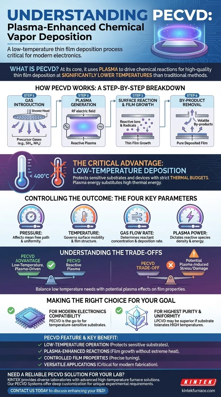
At its core, Plasma-Enhanced Chemical Vapor Deposition (PECVD) is a process used to deposit high-quality thin films onto a material, known as a substrate. It leverages an energized gas, or plasma, to drive the chemical reactions necessary for film growth, allowing the entire process to occur at significantly lower temperatures than traditional methods.
The fundamental advantage of PECVD is its ability to substitute high thermal energy with plasma energy. This allows for the creation of robust thin films on substrates that cannot withstand high temperatures, making it a critical technology in modern electronics fabrication.
How PECVD Works: A Step-by-Step Breakdown
The PECVD process takes place inside a controlled vacuum chamber. Understanding the sequence of events reveals how it achieves low-temperature deposition.
Step 1: Gas Introduction
Precursor gases, such as silane (SiH4) or ammonia (NH3), are introduced into the vacuum chamber. These gases contain the atoms required for the final film. They often flow through a perforated plate, or "shower head," to ensure even distribution over the substrate.
Step 2: Plasma Generation
A powerful radio frequency (RF) electric field is applied between two electrodes inside the chamber. This field energizes the precursor gases, stripping electrons from their atoms and creating a glowing, chemically reactive plasma.
Step 3: Surface Reaction and Film Growth
This plasma contains highly reactive ions and radicals that traditional processes can only create at extreme temperatures. These reactive species diffuse to the substrate's surface, where they react, bond, and build up layer-by-layer to form the desired solid thin film.
Step 4: By-product Removal
The chemical reactions on the surface also create volatile by-products. These are continuously pumped out of the vacuum chamber, leaving behind only the pure, deposited film.
The Critical Advantage: Low-Temperature Deposition
The primary reason for PECVD's widespread adoption is its low operating temperature. Many advanced semiconductor devices have strict thermal budgets, meaning they can be damaged or destroyed if exposed to the high heat required by older furnace-based deposition methods.
Because the plasma provides the energy needed to break down the precursor gases, the substrate itself can remain at a much lower temperature (often below 400°C). This circumvents the need for high thermal energy and protects sensitive, pre-existing components on an integrated circuit.
Controlling the Outcome: The Four Key Parameters
The final properties of the deposited film—such as its thickness, density, and chemical composition—are directly controlled by four critical process parameters.
Pressure
The pressure inside the chamber affects the mean free path of gas molecules, or how far they travel before colliding. Lower pressure can influence how uniformly the reactive species reach the substrate.
Temperature
While lower than other methods, the substrate temperature is still a crucial variable. It governs the surface mobility of the deposited atoms, influencing how they arrange themselves and affecting the final film's structure and quality.
Gas Flow Rate
The rate at which precursor gases are supplied determines the concentration of reactants available in the chamber. This directly impacts the deposition rate and the stoichiometry of the film.
Plasma Power
The power applied to generate the plasma dictates the density and energy of the reactive species. Higher power increases the reaction energy, which can speed up deposition but also potentially cause damage to the substrate if not carefully controlled.
Understanding the Trade-offs
While powerful, PECVD is not a universal solution. Its main advantage—the use of plasma—is also the source of its primary trade-off.
The energetic ion bombardment that enables low-temperature deposition can sometimes induce stress or cause minor physical damage to the substrate or the growing film. For applications demanding the absolute highest level of crystalline perfection or the lowest possible interface defects, a higher-temperature process like Low-Pressure Chemical Vapor Deposition (LPCVD) might still be preferred if the thermal budget allows.
Ultimately, the choice involves balancing the need for low temperature against the potential for plasma-induced effects on the film's final properties.
Making the Right Choice for Your Goal
Selecting a deposition method requires aligning the process capabilities with your primary objective.
- If your primary focus is compatibility with modern electronics: PECVD is the go-to choice for depositing films on temperature-sensitive substrates or devices with tight thermal budgets.
- If your primary focus is achieving the highest possible film purity and uniformity: A furnace-based process like LPCVD may be superior, but only if your substrate can tolerate the significantly higher processing temperatures.
By using plasma to drive chemical reactions, PECVD provides an indispensable tool for building the complex, multi-layered structures found in today's technology.
Summary Table:
| PECVD Feature | Key Benefit |
|---|---|
| Low-Temperature Operation | Protects temperature-sensitive substrates and devices. |
| Plasma-Enhanced Reactions | Enables film growth without extreme heat. |
| Controlled Film Properties | Precise tuning of thickness, density, and composition. |
| Versatile Applications | Critical for modern semiconductor and electronics fabrication. |
Need a reliable PECVD solution for your lab?
Leveraging exceptional R&D and in-house manufacturing, KINTEK provides diverse laboratories with advanced high-temperature furnace solutions. Our product line, including PECVD Systems, is complemented by our strong deep customization capability to precisely meet your unique experimental requirements for low-temperature thin film deposition.
Contact us today to discuss how our PECVD systems can enhance your research and development!
Visual Guide
Related Products
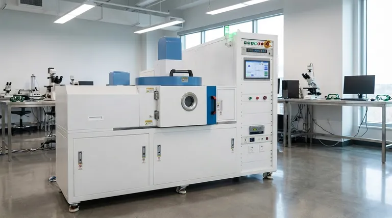
- RF PECVD System Radio Frequency Plasma Enhanced Chemical Vapor Deposition
- Slide PECVD Tube Furnace with Liquid Gasifier PECVD Machine
- Inclined Rotary Plasma Enhanced Chemical Deposition PECVD Tube Furnace Machine
- Inclined Rotary Plasma Enhanced Chemical Deposition PECVD Tube Furnace Machine
- Cylindrical Resonator MPCVD Machine System for Lab Diamond Growth
People Also Ask
- How is silicon dioxide deposited from tetraethylorthosilicate (TEOS) in PECVD? Achieve Low-Temperature, High-Quality SiO2 Films
- What are some promising applications of PECVD-prepared 2D materials? Unlock Advanced Sensing and Optoelectronics
- What are the advantages of PECVD in film deposition? Achieve Low-Temp, High-Quality Coatings
- What is RF in PECVD? A Critical Control for Plasma Deposition
- What are the applications of plasma enhanced chemical vapor deposition? Key Uses in Electronics, Optics & Materials


