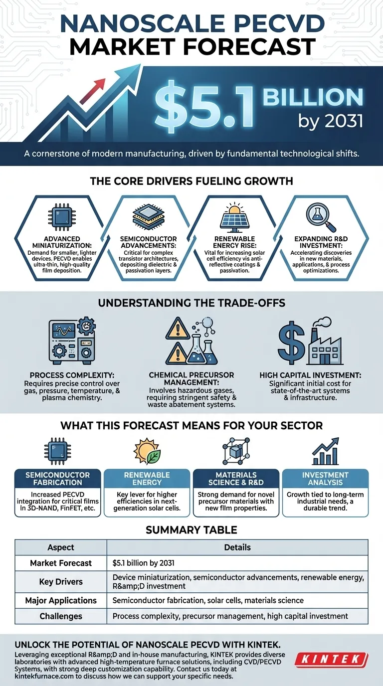
The market forecast for nanoscale PECVD indicates significant expansion, with projections showing the market reaching $5.1 billion by 2031. This growth is not speculative; it is firmly rooted in fundamental technological shifts across major global industries, including the relentless push for device miniaturization and critical advancements in semiconductors and renewable energy.
The core takeaway is that Plasma-Enhanced Chemical Vapor Deposition (PECVD) at the nanoscale is evolving from a specialized laboratory technique into a cornerstone of modern manufacturing. Its growth is a direct reflection of the global demand for smaller, more powerful, and more efficient electronic and energy components.
The Core Drivers Fueling Market Growth
The $5.1 billion forecast is underpinned by several powerful and interconnected industry trends. Understanding these drivers is key to grasping the market's long-term stability and strategic importance.
The Push for Advanced Miniaturization
The demand for smaller, lighter, and more powerful devices in sectors like consumer electronics, medical technology, and IoT is relentless. Nanoscale PECVD is essential for this trend.
It allows for the deposition of extremely thin, uniform, and high-quality films, which are the building blocks of miniaturized components. This precision is impossible to achieve with many older, bulkier deposition methods.
Advancements in Semiconductor Manufacturing
The semiconductor industry is a primary consumer of nanoscale PECVD technology. As chip manufacturers push the boundaries of Moore's Law, they require new methods to build complex, multi-layered transistor architectures.
PECVD is critical for depositing the dielectric layers that insulate conductive paths and for the passivation layers that protect the chip's surface. Its ability to operate at lower temperatures also prevents damage to sensitive, pre-existing structures on the wafer.
The Rise of Renewable Energy
In the renewable energy sector, specifically photovoltaics, nanoscale PECVD plays a vital role in increasing efficiency.
It is used to apply anti-reflective coatings and passivation layers to silicon solar cells. These ultra-thin films reduce energy loss from reflection and improve the cell's ability to convert sunlight into electricity, directly contributing to more powerful and cost-effective solar panels.
Expanding Investment in Research & Development
A positive feedback loop is accelerating the market. As industries recognize the value of PECVD, they increase R&D funding to explore new materials, applications, and process optimizations.
This investment leads to new discoveries—such as novel precursors or applications in flexible electronics—which in turn creates new market opportunities and drives further adoption.
Understanding the Trade-offs
While the outlook is strong, PECVD is not a universally simple solution. Adopting this technology involves navigating specific technical and operational challenges.
Process Complexity and Control
Nanoscale PECVD is a highly sophisticated process. Achieving consistent, high-quality film deposition requires precise control over numerous variables, including gas flow, pressure, temperature, and plasma chemistry.
This complexity demands significant process expertise and advanced monitoring equipment to maintain high yields in a production environment.
Chemical Precursor Management
The precursor gases used in PECVD can be hazardous, flammable, or toxic. Their use necessitates stringent safety protocols, specialized handling infrastructure, and robust waste abatement systems.
These safety and environmental requirements add to the overall operational cost and complexity of running a fabrication facility that relies on PECVD.
High Capital Investment
State-of-the-art PECVD systems, particularly those designed for high-volume manufacturing in industries like semiconductors, represent a significant capital expenditure.
This high initial cost can be a barrier to entry for smaller companies or research institutions, though the long-term return on investment is often justified by the enhanced device performance and manufacturing capabilities.
What This Forecast Means for Your Sector
The growth of nanoscale PECVD is not uniform; its impact will be felt differently across various sectors. Here is how to interpret this trend based on your specific goals.
- If your primary focus is semiconductor fabrication: Expect increased integration of PECVD for depositing critical films in 3D-NAND, FinFET, and other advanced logic and memory architectures.
- If your primary focus is renewable energy: This technology is a key lever for achieving higher efficiencies in next-generation solar cells, making it a critical area for innovation and manufacturing investment.
- If your primary focus is materials science or R&D: The market's expansion signals a strong demand for novel precursor materials that can enable new film properties or lower deposition temperatures.
- If your primary focus is investment analysis: The market's growth is tied to fundamental, long-term industrial needs, suggesting it is a durable trend rather than a short-term bubble.
Understanding these dynamics allows you to strategically position your efforts within this critical and expanding technological landscape.
Summary Table:
| Aspect | Details |
|---|---|
| Market Forecast | $5.1 billion by 2031 |
| Key Drivers | Device miniaturization, semiconductor advancements, renewable energy, R&D investment |
| Major Applications | Semiconductor fabrication, solar cells, materials science |
| Challenges | Process complexity, precursor management, high capital investment |
Unlock the Potential of Nanoscale PECVD with KINTEK
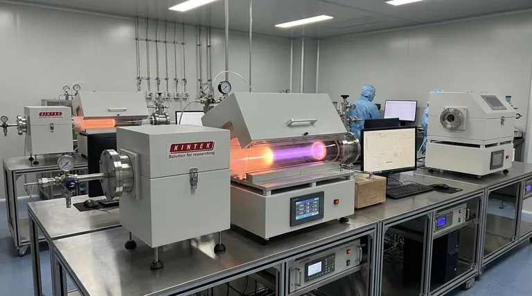
Leveraging exceptional R&D and in-house manufacturing, KINTEK provides diverse laboratories with advanced high-temperature furnace solutions. Our product line, including Muffle, Tube, Rotary Furnaces, Vacuum & Atmosphere Furnaces, and CVD/PECVD Systems, is complemented by our strong deep customization capability to precisely meet unique experimental requirements.
Whether you're in semiconductor fabrication, renewable energy, or materials R&D, our tailored PECVD solutions can enhance your efficiency, improve film quality, and accelerate innovation. Contact us today to discuss how we can support your specific needs and drive your projects forward!
Visual Guide
Related Products
- Inclined Rotary Plasma Enhanced Chemical Deposition PECVD Tube Furnace Machine
- Inclined Rotary Plasma Enhanced Chemical Deposition PECVD Tube Furnace Machine
- RF PECVD System Radio Frequency Plasma Enhanced Chemical Vapor Deposition
- Slide PECVD Tube Furnace with Liquid Gasifier PECVD Machine
- HFCVD Machine System Equipment for Drawing Die Nano Diamond Coating
People Also Ask
- What types of materials can be processed in rotary tube furnaces? Optimize Your Thermal Processing with Versatile Solutions
- What are the main advantages of PECVD tube furnaces compared to CVD tube furnaces? Lower Temp, Faster Deposition, and More
- What plasma source is used in PE-CVD tube furnaces? Unlock Low-Temperature, High-Quality Deposition
- What optional features enhance the processing capabilities of rotary tube furnaces? Boost Efficiency with Advanced Customizations
- How does the temperature control system work in a rotary tube furnace? Achieve Precise Thermal Processing for Your Materials


