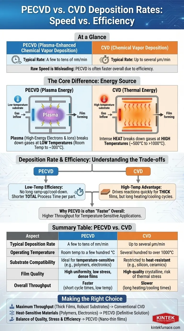
At a glance, conventional Chemical Vapor Deposition (CVD) generally offers a higher maximum deposition rate, capable of reaching several micrometers per minute. In contrast, Plasma-Enhanced Chemical Vapor Deposition (PECVD) typically operates in the range of a few to tens of nanometers per minute. However, this simple speed comparison is misleading; PECVD's lower operating temperature often makes it a more efficient and faster overall process for many modern applications.
The choice between PECVD and CVD is not about which is universally "faster." It's a fundamental trade-off between using high heat (CVD) versus plasma energy (PECVD) to create a film, a decision that profoundly impacts temperature, film quality, and substrate compatibility.
The Core Difference: Thermal vs. Plasma Energy
To understand the difference in rates and performance, you must first understand the mechanism each process uses to supply the energy needed for deposition.
How Conventional CVD Works
Conventional CVD relies purely on thermal energy. Precursor gases are introduced into a high-temperature chamber (often several hundred to over 1000°C). This intense heat breaks down the gas molecules, allowing them to react and deposit as a solid thin film on the substrate's surface.
How PECVD Works
PECVD bypasses the need for extreme heat by using an electric field to create plasma, an ionized gas containing high-energy electrons and ions. This plasma provides the activation energy to break down the precursor gases at much lower temperatures, from room temperature to a few hundred degrees Celsius.
Deposition Rate: More Than Just Speed
The deposition rate is a direct consequence of the energy source. While one method can achieve a higher peak speed, the other is often more practical and efficient.
CVD's High-Temperature Advantage
Because it uses high thermal energy, CVD can drive chemical reactions very quickly, enabling very high deposition rates. This makes it suitable for applications where thick films (several micrometers or more) are needed and the substrate can tolerate the extreme temperatures.
PECVD's Low-Temperature Efficiency
PECVD's rate is limited by the plasma density and gas flow, but its true advantage lies in its efficiency. By operating at low temperatures, it eliminates the long ramp-up and cool-down times required for high-temperature CVD furnaces. This dramatically shortens the total process time per wafer or part.
Why PECVD Is Often Considered "Faster"
When sources claim PECVD is faster, they are usually referring to the overall throughput. For temperature-sensitive materials like electronics or polymers, CVD is not an option. Compared to other low-temperature methods, or when factoring in the total cycle time, PECVD often provides a faster and more cost-effective path to a finished product.
Understanding the Trade-offs
The choice between CVD and PECVD involves balancing several critical factors beyond just the deposition rate.
Film Quality and Stress
PECVD's low processing temperature significantly reduces thermal stress on the film and substrate. This results in films with excellent uniformity, high density, and fewer pinholes, which is critical for nano-scale electronic and optical layers.
High-temperature CVD can also produce very high-quality crystalline films, but it risks introducing thermal stress, defects, or lattice mismatch, especially when depositing on a material with a different thermal expansion coefficient.
Substrate Compatibility
This is often the deciding factor. PECVD is ideal for depositing films on temperature-sensitive substrates that would be damaged or destroyed by conventional CVD temperatures. This includes polymers, plastics, and complex electronic devices with existing circuitry.
CVD is restricted to materials that can withstand high heat, such as silicon wafers, ceramics, and certain metals.
Cost and Complexity
Conventional CVD can be costly due to its high energy consumption and expensive precursors. The long cycle times for heating and cooling also limit its operational efficiency.
PECVD can be more cost-effective due to its faster overall cycle times and ability to use cheaper precursor materials. This makes it highly suitable for large-scale manufacturing where throughput is key.
Film Properties and Limitations
PECVD is highly tailorable, allowing for the creation of films with specific properties like hydrophobicity or UV protection. However, these plasma-deposited films can be softer and have lower wear resistance than some hard coatings produced by other methods.
Making the Right Choice for Your Goal
Selecting the correct deposition method requires matching the process capabilities to your specific technical and business objectives.
- If your primary focus is maximum throughput for thick films on robust substrates: Conventional CVD may be the right choice for its high raw deposition rate, provided the material can handle the heat.
- If your primary focus is depositing on heat-sensitive materials like polymers or electronics: PECVD is the definitive and often only viable solution due to its low-temperature process.
- If your primary focus is a balance of film quality, stress control, and overall efficiency: PECVD often provides the most effective solution, particularly for creating high-performance, nano-thin films in a production environment.
Ultimately, the best method is the one that aligns with your material constraints, film quality requirements, and production goals.
Summary Table:
| Aspect | PECVD | CVD |
|---|---|---|
| Typical Deposition Rate | A few to tens of nm/min | Up to several μm/min |
| Operating Temperature | Room temp to a few hundred °C | Several hundred to over 1000°C |
| Substrate Compatibility | Ideal for temperature-sensitive materials (e.g., polymers, electronics) | Restricted to heat-resistant materials (e.g., silicon, ceramics) |
| Film Quality | High uniformity, low stress, dense films | High-quality crystalline films, risk of thermal stress |
| Overall Throughput | Faster due to low temp and short cycle times | Slower due to long heating/cooling times |
Struggling to choose the right deposition method for your lab's unique needs? At KINTEK, we specialize in advanced high-temperature furnace solutions, including our CVD/PECVD Systems, designed to deliver precise, efficient thin-film deposition. Leveraging our exceptional R&D and in-house manufacturing, we offer deep customization to meet your specific experimental requirements—whether you need high throughput, low-temperature processing, or superior film quality. Don't let process limitations hold you back—contact us today to discuss how our tailored solutions can enhance your research and production outcomes!
Visual Guide
Related Products
- Slide PECVD Tube Furnace with Liquid Gasifier PECVD Machine
- RF PECVD System Radio Frequency Plasma Enhanced Chemical Vapor Deposition
- Inclined Rotary Plasma Enhanced Chemical Deposition PECVD Tube Furnace Machine
- Inclined Rotary Plasma Enhanced Chemical Deposition PECVD Tube Furnace Machine
- Multi Heating Zones CVD Tube Furnace Machine for Chemical Vapor Deposition Equipment
People Also Ask
- How does PECVD equipment contribute to TOPCon bottom cells? Mastering Hydrogenation for Maximum Solar Efficiency
- What are the advantages of using a tube furnace CVD system for Cu(111)/graphene? Superior Scalability and Quality
- What is plasma in the context of PECVD? Unlock Low-Temperature Thin Film Deposition
- What role does a Tube Furnace play in the CVD growth of carbon nanotubes? Achieve High-Purity CNT Synthesis
- How does a hydrogen reduction environment in an industrial tube furnace facilitate gold-copper alloy microspheres?


