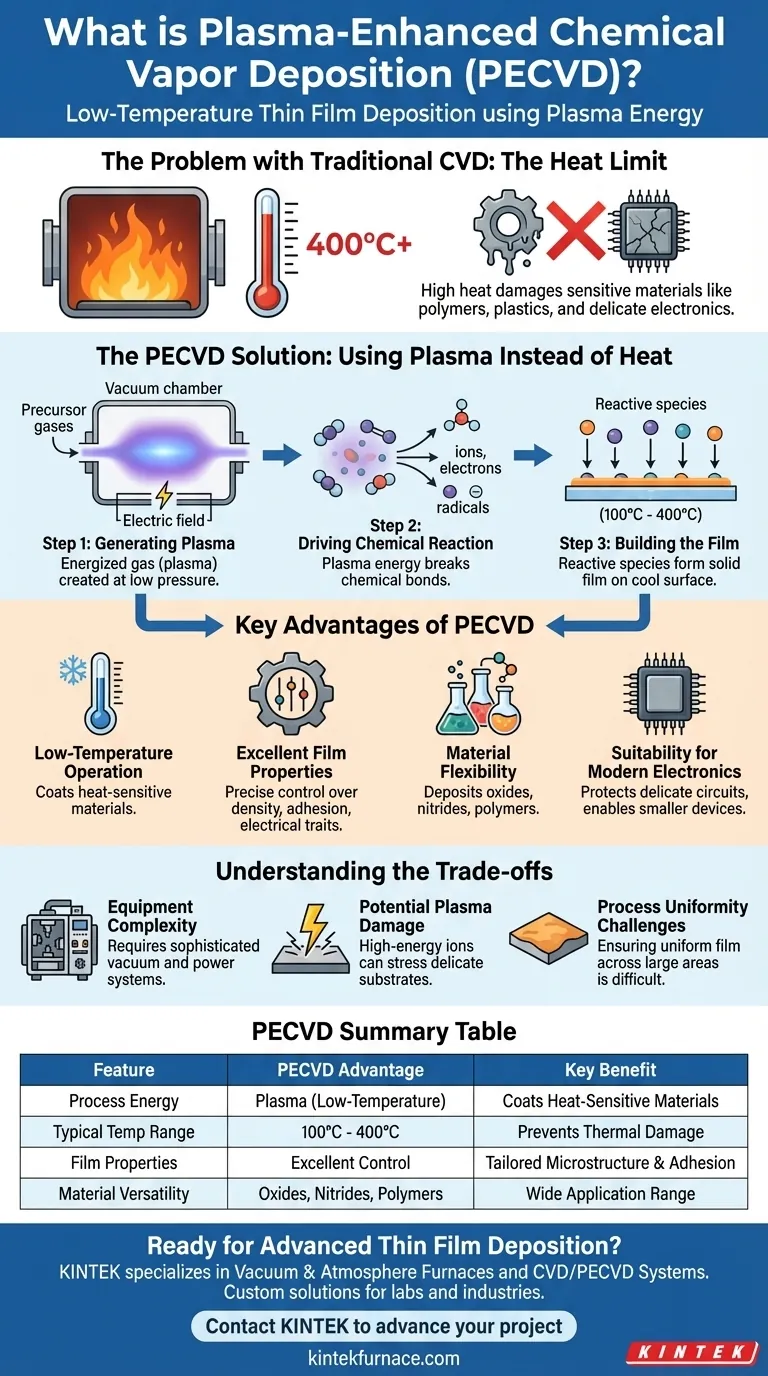
At its core, Plasma-Enhanced Chemical Vapor Deposition (PECVD) is an advanced process for creating very thin films of material on a surface. Unlike traditional methods that rely on intense heat, PECVD uses an energized gas, or plasma, to drive the chemical reactions needed to build the film layer by layer. This allows for deposition at significantly lower temperatures.
The fundamental problem with many material coating processes is their reliance on high temperatures, which damages or destroys sensitive substrates like plastics and delicate electronics. PECVD solves this by using plasma to provide the necessary reaction energy, unlocking the ability to deposit high-performance films on a much wider range of materials.
The Problem PECVD Solves: The Limits of Heat
Why Traditional Deposition is Restrictive
Traditional Chemical Vapor Deposition (CVD) works by heating a substrate to a very high temperature within a chamber filled with precursor gases.
This thermal energy breaks the chemical bonds in the gas molecules, allowing them to react and deposit as a solid film on the hot surface.
The Temperature Constraint
The high temperatures required for traditional CVD (often well above 400°C) make it completely unsuitable for coating materials with low melting points.
This includes common polymers, plastics, and complex microelectronic devices that would be damaged or destroyed by the heat. This severely limits innovation in fields that rely on these materials.
How PECVD Works: Using Plasma Instead of Heat
Step 1: Generating the Plasma
The PECVD process begins by placing a substrate in a low-pressure vacuum chamber. Precursor gases are introduced, but instead of applying intense heat, an electric field is used to energize the gas.
This process, often using a capacitive glow discharge, strips electrons from the gas atoms, creating a plasma—an ionized gas containing a mix of ions, electrons, and highly reactive neutral particles.
Step 2: Driving the Chemical Reaction
This plasma provides the energy needed to break down the precursor gas molecules into reactive groups.
These highly reactive components then move to the substrate surface, which is kept at a much lower temperature (typically 100°C to 400°C).
Step 3: Building the Film
On the cooler substrate surface, these reactive species combine and settle, forming a dense, high-quality solid film.
The thickness of this film can be precisely controlled, ranging from just a few nanometers up to several micrometers.
Key Advantages of the PECVD Method
Substrate Versatility
The single most important advantage of PECVD is its low-temperature operation. This makes it possible to deposit high-performance coatings on temperature-sensitive materials that were previously impossible to coat.
Excellent Film Properties
PECVD allows for precise control over the plasma's density and energy. This gives engineers fine-tuned control over the deposited film's properties, such as its microstructure, density, electrical characteristics, and adhesion to the substrate.
Material Flexibility
The process is incredibly versatile and can be used to deposit a wide range of materials. This includes critical compounds like oxides, nitrides, and even some polymers, offering significant flexibility for designing catalysts, semiconductors, and protective coatings.
Suitability for Modern Electronics
As microelectronic components shrink, they become more vulnerable to heat. The low temperatures of PECVD prevent damage to delicate circuits and provide better control over dopant placement, a critical factor for high-performance devices.
Understanding the Trade-offs
Equipment Complexity
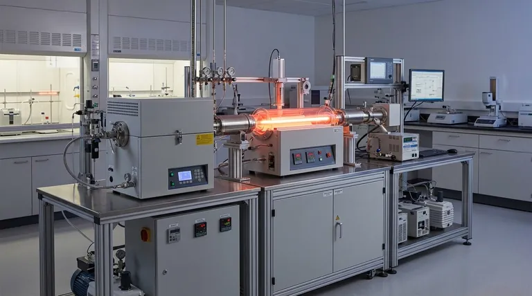
PECVD systems are inherently more complex than simple thermal CVD reactors. They require sophisticated vacuum pumps, radio-frequency (RF) power supplies, and impedance matching networks to generate and control the plasma, which can increase initial costs.
Potential for Plasma-Induced Damage
While far gentler than high heat, the high-energy ions within the plasma can sometimes cause subtle physical damage or stress to the surface of the most delicate substrates if the process is not perfectly tuned.
Process Uniformity Challenges
Generating a perfectly uniform plasma over a large surface area is a significant engineering challenge. Any non-uniformity in the plasma can lead to variations in the thickness and properties of the deposited film across the substrate.
Making the Right Choice for Your Application
Choosing a deposition method depends entirely on your project's constraints and goals.
- If your primary focus is coating heat-sensitive materials like polymers or plastics: PECVD is the definitive and often only viable choice due to its low-temperature operation.
- If your primary focus is maximum film quality on a robust, heat-tolerant substrate: Traditional CVD can sometimes produce films with higher crystallinity, though PECVD offers greater control over other properties.
- If your primary focus is versatility and scalability for advanced electronics or catalysts: PECVD provides an unmatched combination of material flexibility, high deposition rates, and precise control for modern industrial applications.
By substituting plasma for heat, PECVD fundamentally expands the frontier of what is possible in materials science and engineering.
Summary Table:
| Feature | PECVD Advantage |
|---|---|
| Process Energy | Plasma (Low-Temperature) |
| Typical Temperature Range | 100°C - 400°C |
| Key Benefit | Coats Heat-Sensitive Materials (e.g., plastics, electronics) |
| Film Properties | Excellent control over density, adhesion, and electrical characteristics |
| Material Versatility | Deposits oxides, nitrides, and polymers |
Ready to integrate low-temperature, high-performance thin film deposition into your R&D or production?
KINTEK specializes in advanced Vacuum & Atmosphere Furnaces and CVD/PECVD Systems. Leveraging our exceptional R&D and in-house manufacturing, we provide robust solutions tailored for laboratories and industries working with sensitive substrates. Our strong deep customization capability ensures your unique experimental and production requirements for catalysts, semiconductors, and protective coatings are met precisely.
Contact KINTEK today to discuss how our PECVD expertise can advance your project.
Visual Guide
Related Products
- Slide PECVD Tube Furnace with Liquid Gasifier PECVD Machine
- RF PECVD System Radio Frequency Plasma Enhanced Chemical Vapor Deposition
- Inclined Rotary Plasma Enhanced Chemical Deposition PECVD Tube Furnace Machine
- Inclined Rotary Plasma Enhanced Chemical Deposition PECVD Tube Furnace Machine
- Multi Heating Zones CVD Tube Furnace Machine for Chemical Vapor Deposition Equipment
People Also Ask
- How does PECVD equipment contribute to TOPCon bottom cells? Mastering Hydrogenation for Maximum Solar Efficiency
- How does a hydrogen reduction environment in an industrial tube furnace facilitate gold-copper alloy microspheres?
- What are the disadvantages of tube furnace cracking when processing heavy raw materials? Avoid Costly Downtime and Inefficiency
- What are the typical conditions for plasma-enhanced CVD processes? Achieve Low-Temperature Thin Film Deposition
- What is plasma in the context of PECVD? Unlock Low-Temperature Thin Film Deposition


