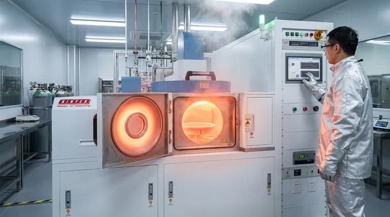
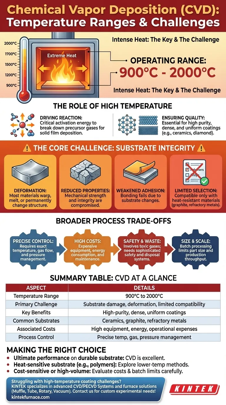
In Chemical Vapor Deposition (CVD), the process operates at extremely high temperatures, typically ranging from 900°C to 2000°C. This intense heat is fundamental to initiating the necessary chemical reactions but also introduces the primary challenge of the process: it severely limits which materials can be used as a substrate without being damaged or destroyed.
The core challenge of CVD is a direct trade-off. The same high temperatures that produce exceptionally pure and high-performance coatings are also high enough to cause structural deformation, weaken mechanical properties, and compromise the integrity of many substrate materials.
The Role of High Temperature in CVD
The extreme temperatures in a CVD process are not an incidental byproduct; they are a necessary component for achieving the desired outcome. This heat provides the critical activation energy for the chemical reactions to occur.
Driving the Chemical Reaction
Precursor gases are introduced into the CVD chamber in a stable state. The high temperature provides the energy needed to break them down and cause them to react, depositing a solid, thin film onto the surface of the substrate.
Ensuring High Film Quality
For many high-performance materials like ceramics, diamond coatings, and other advanced films, high temperatures are essential for creating a final product that is highly pure, dense, and uniform with exceptional properties.
The Core Challenge: Substrate Integrity
The primary limitation of CVD stems directly from its high operating temperature. Only materials that are thermally stable within the 900°C to 2000°C range can be successfully coated.
Deformation and Structural Changes
Most materials will deform, warp, or melt at these temperatures. Even if a substrate does not melt, the heat can cause permanent changes to its internal crystalline structure, altering its fundamental characteristics.
Reduced Mechanical Properties
These structural changes often lead to a reduction in the base material's mechanical properties. A substrate may become more brittle or lose its tensile strength after being subjected to the CVD process.
Weakened Coating Adhesion
If the substrate deforms or changes its structure during deposition, the bond between the coating and the base material can be severely weakened. This can lead to the coating flaking or peeling off, defeating the purpose of the process.
Limited Material Selection
The direct consequence is a drastic limitation on substrate choice. The process is best suited for coating materials that are already highly resistant to heat, such as certain ceramics, graphite, or refractory metals. It is incompatible with most polymers and many common metal alloys.
Understanding the Broader Process Trade-offs
The high-temperature requirement creates a cascade of related challenges that define the practical application of CVD. Anyone considering this process must weigh these factors carefully.
Precise Process Control
The temperature is not the only critical variable. It must be controlled with extreme precision in conjunction with gas flow rates and chamber pressure. Any deviation can lead to defects in the final film, wasting a costly and complex production run.
High Equipment and Operational Costs
Building and maintaining a system capable of safely handling extreme temperatures, vacuum conditions, and reactive gases is expensive. The energy consumption required to sustain temperatures up to 2000°C contributes significantly to high operational costs.
Safety and Waste Management
CVD often involves toxic, flammable, or corrosive precursor gases. The high-temperature environment increases the risks, necessitating sophisticated safety protocols and effective exhaust and waste management systems to protect personnel and the environment.
Size and Scale Constraints
The specialized, high-temperature reaction chambers restrict the size and quantity of parts that can be coated at one time. This batch-processing nature can limit throughput and increase lead times for large-scale production.
Making the Right Choice for Your Application
Choosing a deposition technology requires balancing the desired coating performance against the physical limitations of your substrate and the economic realities of your project.
- If your primary focus is ultimate coating performance on a durable substrate: CVD is an excellent choice for creating superior, high-purity films, provided your substrate material can withstand operating temperatures between 900°C and 2000°C.
- If your substrate is heat-sensitive (e.g., polymers, aluminum, some steels): You must explore lower-temperature deposition methods, as standard high-temperature CVD will almost certainly damage or destroy the part.
- If your project is highly cost-sensitive or requires high-volume production: Carefully evaluate the high capital and operational costs, as well as the batch-processing limitations of CVD, against your manufacturing goals.
Understanding the thermal limitations of Chemical Vapor Deposition is the first and most critical step in determining its feasibility for your project.
Summary Table:
| Aspect | Details |
|---|---|
| Temperature Range | 900°C to 2000°C |
| Primary Challenge | Substrate damage, deformation, and limited material compatibility |
| Key Benefits | High-purity, dense, and uniform coatings for advanced materials |
| Common Substrates | Ceramics, graphite, refractory metals (heat-resistant materials) |
| Associated Costs | High equipment, energy, and operational expenses |
| Process Control | Requires precise temperature, gas flow, and pressure management |
Struggling with high-temperature coating challenges? KINTEK specializes in advanced high-temperature furnace solutions, including our reliable CVD/PECVD Systems. Leveraging exceptional R&D and in-house manufacturing, we offer deep customization to meet your unique experimental needs with products like Muffle, Tube, Rotary, Vacuum & Atmosphere Furnaces. Enhance your lab's efficiency and achieve superior results—contact us today to discuss how we can support your project!
Visual Guide
Related Products
- Custom Made Versatile CVD Tube Furnace Chemical Vapor Deposition CVD Equipment Machine
- Split Chamber CVD Tube Furnace with Vacuum Station CVD Machine
- Multi Heating Zones CVD Tube Furnace Machine for Chemical Vapor Deposition Equipment
- Slide PECVD Tube Furnace with Liquid Gasifier PECVD Machine
- Inclined Rotary Plasma Enhanced Chemical Deposition PECVD Tube Furnace Machine
People Also Ask
- What are the key application fields of CVD tube furnaces? Unlock Precision in Thin-Film Synthesis
- How does CVD tube furnace sintering enhance graphene growth? Achieve Superior Crystallinity and High Electron Mobility
- What temperature range do standard CVD tube furnaces operate at? Unlock Precision for Your Material Deposition
- Which industries and research fields benefit from CVD tube furnace sintering systems for 2D materials? Unlock Next-Gen Tech Innovations
- Why are CVD tube furnace sintering systems indispensable for 2D material research and production? Unlock Atomic-Scale Precision


