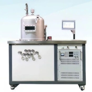
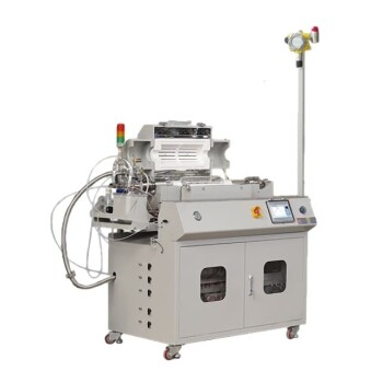
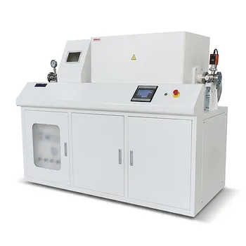
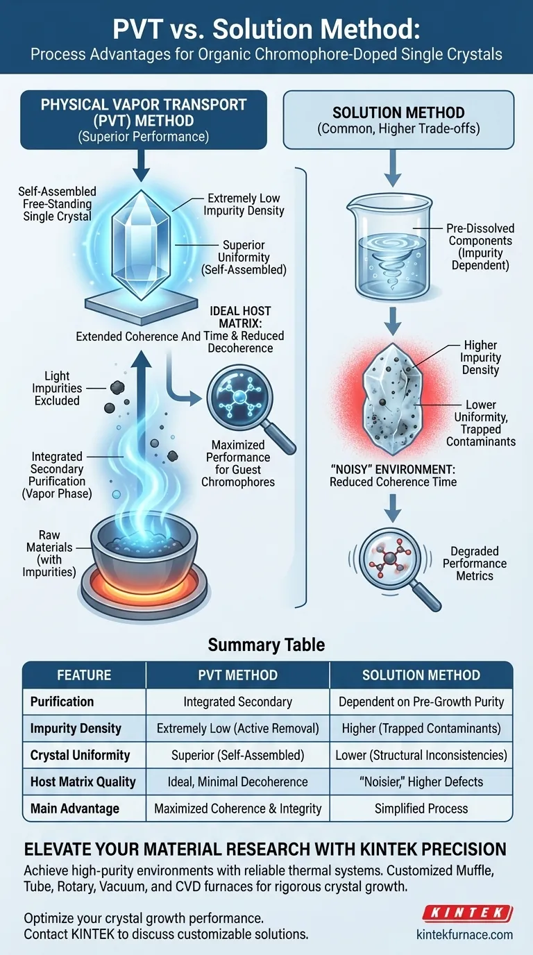
The Physical Vapor Transport (PVT) method distinguishes itself by integrating a secondary purification mechanism directly into the crystal growth process. Unlike the solution method, PVT effectively separates light impurities from the raw materials, resulting in self-assembled free-standing organic single crystals with superior uniformity. This process yields an extremely low impurity density, creating an optimized host matrix that is essential for extending the coherence time of the molecular system.
While solution-based methods are common, PVT offers a distinct advantage by coupling growth with purification. This results in a highly uniform host matrix that minimizes impurity-driven decoherence, making it the superior choice for high-performance applications.
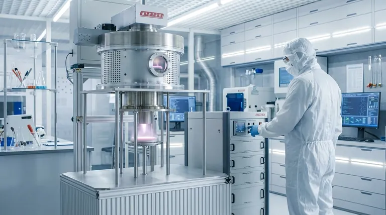
The Purification Advantage
Integrated Secondary Purification
The most significant process advantage of PVT is its ability to perform secondary purification simultaneously with crystal growth.
While the solution method relies on the purity of the pre-dissolved components, PVT actively filters the material as it transitions phases. This ensures that the final crystal structure is not compromised by contaminants present in the raw stock.
Elimination of Light Impurities
PVT is particularly effective at separating light impurities from the source material.
By leveraging the differences in vapor transport properties, light impurities are excluded from the growing crystal lattice. This leads to a level of chemical purity that is difficult to achieve through standard solution processing.
Structural Superiority Over Solution Methods
Enhanced Uniformity
When compared to Metal-Organic Frameworks (MOFs) prepared via the solution method, crystals grown via PVT exhibit significantly higher uniformity.
The self-assembly nature of the free-standing crystals in the vapor phase prevents the structural inconsistencies often found in solution-grown counterparts. This uniformity is critical for applications requiring consistent physical properties across the entire crystal volume.
Creating the Ideal Host Matrix
The combination of high uniformity and extremely low impurity density creates an ideal host matrix for guest molecules.
In doped systems, the quality of the host lattice directly dictates the performance of the guest chromophores. A cleaner, more uniform PVT-grown matrix allows these molecules to integrate with fewer defects.
Understanding the Operational Trade-offs
The Cost of Impurities in Solution Methods
The primary pitfall of choosing the solution method over PVT is the retention of impurities.
In solution-based growth, contaminants often become trapped within the lattice or the solvent inclusions. This results in a "noisy" environment for the guest molecules, which directly degrades performance metrics.
Impact on Coherence Time
The ultimate trade-off involves the coherence time of the molecular system.
Crystals with higher impurity densities and lower uniformity—typical of solution methods—suffer from reduced coherence. If your application relies on long coherence times, the solution method represents a significant performance compromise compared to PVT.
Making the Right Choice for Your Goal
To maximize the performance of organic chromophore-doped crystals, evaluate your specific requirements against the capabilities of PVT.
- If your primary focus is maximizing coherence time: Prioritize PVT to ensure the lowest possible impurity density and reduce environmental noise around the guest molecules.
- If your primary focus is structural consistency: Utilize PVT to achieve high uniformity and avoid the structural defects common in solution-grown MOFs.
Select the PVT method when the integrity of the host matrix is non-negotiable for the success of your molecular system.
Summary Table:
| Feature | Physical Vapor Transport (PVT) | Solution Method |
|---|---|---|
| Purification | Integrated secondary purification during growth | Dependent on pre-growth material purity |
| Impurity Density | Extremely low; active removal of light impurities | Higher; contaminants often trapped in lattice |
| Crystal Uniformity | Superior; self-assembled free-standing structures | Lower; prone to structural inconsistencies |
| Host Matrix Quality | Ideal for guest molecules; minimal decoherence | Noisier environment; higher defect density |
| Main Advantage | Maximized coherence time & structural integrity | Simplified process but higher performance trade-offs |
Elevate Your Material Research with KINTEK Precision
To achieve the high-purity environments required for successful Physical Vapor Transport, you need reliable thermal systems. KINTEK provides industry-leading Muffle, Tube, Rotary, Vacuum, and CVD systems, all backed by expert R&D and manufacturing. Our lab high-temperature furnaces are fully customizable to meet the rigorous demands of organic single crystal growth and impurity-free processing.
Ready to optimize your crystal growth performance? Contact KINTEK today to discuss how our customizable furnace solutions can support your specific research and production goals.
Visual Guide
References
- Ian B. Logue, Bumsu Lee. Ensemble emission of isolated organic chromophores incorporated into an organometallic single crystal. DOI: 10.1515/nanoph-2025-0079
This article is also based on technical information from Kintek Furnace Knowledge Base .
Related Products
- Cylindrical Resonator MPCVD Machine System for Lab Diamond Growth
- MPCVD Machine System Reactor Bell-jar Resonator for Lab and Diamond Growth
- RF PECVD System Radio Frequency Plasma Enhanced Chemical Vapor Deposition
- 915MHz MPCVD Diamond Machine Microwave Plasma Chemical Vapor Deposition System Reactor
- HFCVD Machine System Equipment for Drawing Die Nano Diamond Coating
People Also Ask
- How does MPCVD achieve stable temperature control during diamond growth? Master Precise Thermal Management
- What are the essential components of an MPCVD reactor system? Build a Pristine Environment for High-Purity Materials
- How do carbon-containing groups contribute to diamond growth in the MPCVD method? Unlock High-Quality Diamond Synthesis
- How does pressure affect the MPCVD growth process? Master Plasma Control for Superior Film Quality
- What factors influence the quality of diamond deposition in the MPCVD method? Master the Critical Parameters for High-Quality Diamond Growth