In semiconductor manufacturing, PECVD is primarily used to deposit critical thin films that serve as insulators, protective layers, and functional components within an integrated circuit. The most common applications are the deposition of silicon dioxide (SiO₂) and silicon nitride (Si₃N₄) for dielectric insulation and passivation, as well as creating specialized layers for transistors and interconnects.
The central value of Plasma-Enhanced Chemical Vapor Deposition (PECVD) is not just what it deposits, but how it does it. Its ability to create high-quality films at low temperatures is the key that unlocks the fabrication of complex, multi-layered semiconductor devices without damaging the sensitive structures already built on the wafer.
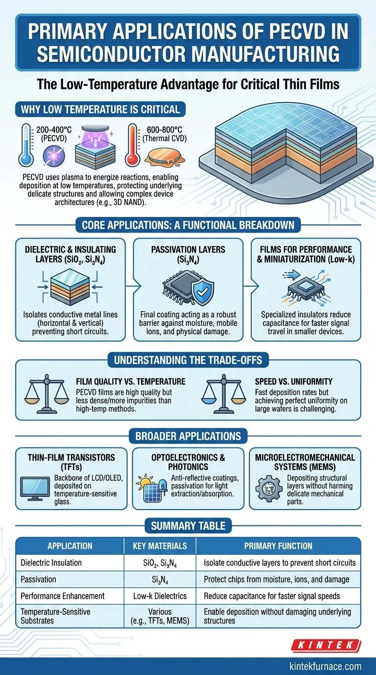
Why Low Temperature is the Critical Advantage
The defining feature of PECVD compared to traditional Chemical Vapor Deposition (CVD) is its use of a plasma to energize the chemical reaction. This allows deposition to occur at significantly lower temperatures (typically 200-400°C) instead of the 600-800°C required for thermal CVD.
Protecting Underlying Structures
Modern chips are built layer by layer. Once you have fabricated temperature-sensitive components like copper interconnects or transistors with specific doping profiles, exposing them to high heat can destroy their structure and electrical properties.
PECVD allows new layers to be added on top of these delicate structures without melting, diffusing, or otherwise damaging them.
Enabling Complex Device Architectures
The low-thermal budget of PECVD is what makes building vertically complex devices, like 3D NAND flash memory or advanced microprocessors, feasible. Each new layer can be deposited without ruining the integrity of the dozens or hundreds of layers beneath it.
The Core Applications: A Functional Breakdown
PECVD isn't a single application but a foundational technique used to create several distinct types of films, each with a specific job.
Dielectric and Insulating Layers
The most common application is depositing silicon dioxide (SiO₂) and silicon nitride (Si₃N₄). These films are excellent electrical insulators.
They are used to isolate conductive metal lines from each other, both horizontally on the same layer and vertically between different layers, preventing short circuits. This is fundamental to the function of any integrated circuit.
Passivation Layers
A passivation layer is the final protective coating applied to a semiconductor chip. Typically made of silicon nitride (Si₃N₄), it acts as a robust barrier.
This layer shields the sensitive circuitry from moisture, mobile ions, and physical damage during packaging and its operational life, directly enhancing device reliability and longevity.
Films for Performance and Miniaturization
As transistors shrink, the distance between components decreases, increasing electrical interference (capacitance) that can slow the chip down.
PECVD is used to deposit low-k dielectric materials. These specialized insulators reduce this unwanted capacitance, allowing signals to travel faster and enabling continued device miniaturization.
Understanding the Trade-offs
While indispensable, PECVD is chosen for a specific balance of properties. It is not a perfect solution for every scenario, and engineers must manage its inherent trade-offs.
Film Quality vs. Temperature
While PECVD films are considered "high quality," they are generally less dense and can have more hydrogen impurities than high-temperature films. For applications demanding the absolute highest purity and stability, such as the critical gate oxide in a transistor, other methods like thermal oxidation are often preferred.
Speed vs. Uniformity
PECVD offers fast deposition rates, which is excellent for manufacturing throughput. However, achieving a perfectly uniform film thickness across a large 300mm wafer can be challenging. Process conditions must be meticulously tuned to balance deposition speed with the required uniformity specifications.
Beyond Standard ICs: Broader Applications
The flexibility of PECVD makes it vital for manufacturing a wide range of other micro-devices.
Thin-Film Transistors (TFTs)
TFTs are the backbone of modern flat-panel displays (LCD, OLED). PECVD is used to deposit the silicon and dielectric layers that form these transistors on large glass substrates, which cannot withstand high temperatures.
Optoelectronics and Photonics
In the production of Light-Emitting Diodes (LEDs) and solar cells, PECVD is used to deposit anti-reflective coatings, passivation layers, and transparent conductive oxides. These films are critical for maximizing light extraction or absorption.
Microelectromechanical Systems (MEMS)
MEMS devices, like accelerometers and micro-mirrors, combine tiny mechanical structures with electronics. PECVD is used to deposit structural layers and sacrificial layers (which are later removed) at temperatures that won't harm the delicate mechanical components.
Making the Right Choice for Your Goal
The specific PECVD film you use is directly tied to its intended function within the device.
- If your primary focus is electrical isolation: PECVD-deposited silicon dioxide (SiO₂) is the industry workhorse for insulating metal layers.
- If your primary focus is final device protection: Silicon nitride (Si₃N₄) is the material of choice for a durable passivation layer due to its excellent barrier properties.
- If your primary focus is high-speed performance: Low-k dielectrics deposited via PECVD are essential for reducing signal delay in advanced logic chips.
- If your primary focus is manufacturing on a temperature-sensitive substrate: PECVD is often the only viable deposition method for devices like flexible electronics or TFTs on glass.
Ultimately, PECVD's low-temperature processing is the enabling technology that allows for the creation of today's complex, reliable, and high-performance semiconductor devices.
Summary Table:
| Application | Key Materials | Primary Function |
|---|---|---|
| Dielectric Insulation | Silicon Dioxide (SiO₂), Silicon Nitride (Si₃N₄) | Isolate conductive layers to prevent short circuits |
| Passivation | Silicon Nitride (Si₃N₄) | Protect chips from moisture, ions, and damage |
| Performance Enhancement | Low-k Dielectrics | Reduce capacitance for faster signal speeds |
| Temperature-Sensitive Substrates | Various (e.g., for TFTs, MEMS) | Enable deposition without damaging underlying structures |
Enhance your semiconductor manufacturing with KINTEK's advanced PECVD systems! Leveraging exceptional R&D and in-house manufacturing, we provide diverse laboratories with high-temperature furnace solutions, including CVD/PECVD Systems, complemented by strong deep customization to precisely meet your unique experimental needs. Contact us today to discuss how our tailored PECVD solutions can improve your device performance and reliability!
Visual Guide
Related Products
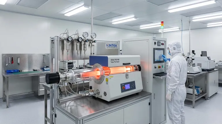
- Slide PECVD Tube Furnace with Liquid Gasifier PECVD Machine
- RF PECVD System Radio Frequency Plasma Enhanced Chemical Vapor Deposition
- Inclined Rotary Plasma Enhanced Chemical Deposition PECVD Tube Furnace Machine
- Inclined Rotary Plasma Enhanced Chemical Deposition PECVD Tube Furnace Machine
- Multi Heating Zones CVD Tube Furnace Machine for Chemical Vapor Deposition Equipment
People Also Ask
- In which industries is the tube furnace commonly used? Essential for Materials Science, Energy, and More
- What role does a Tube Furnace play in the CVD growth of carbon nanotubes? Achieve High-Purity CNT Synthesis
- What are the main advantages of PECVD tube furnaces compared to CVD tube furnaces? Lower Temp, Faster Deposition, and More
- What are the advantages of using a tube furnace CVD system for Cu(111)/graphene? Superior Scalability and Quality
- What plasma source is used in PE-CVD tube furnaces? Unlock Low-Temperature, High-Quality Deposition


