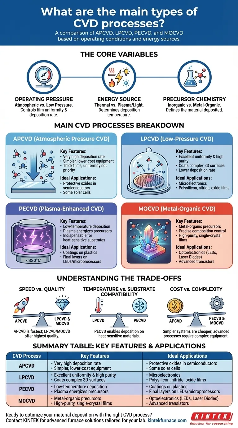
The primary types of Chemical Vapor Deposition (CVD) are defined by their operating conditions and energy sources. The most common classifications are Atmospheric Pressure CVD (APCVD), Low-Pressure CVD (LPCVD), Plasma-Enhanced CVD (PECVD), and Metal-Organic CVD (MOCVD), each engineered to solve a specific set of material deposition challenges.
Choosing a CVD process is not about finding the "best" one, but about understanding the fundamental trade-offs. The decision is a deliberate balance between deposition speed, film quality, processing temperature, and cost, dictated entirely by the requirements of your final application.
The Core Variables That Define a CVD Process
To understand the different types of CVD, you must first grasp the three core variables that engineers manipulate to control the film's properties. These variables are the reason different methods exist.
Operating Pressure
Pressure inside the reaction chamber directly impacts the behavior of precursor gas molecules. It is the primary lever for controlling film uniformity and deposition rate.
At atmospheric pressure, molecules collide frequently, leading to faster reactions in the gas phase but potentially lower uniformity on the substrate. At low pressure, molecules travel further before colliding, which slows the deposition rate but dramatically improves the uniformity and purity of the film across the substrate surface.
Energy Source
A chemical reaction needs energy to initiate. In CVD, this energy can be supplied in several forms, with the choice of source being the most critical factor for determining the required deposition temperature.
Thermal energy is the most traditional source, using heat to break down precursor gases. However, plasma can also be used to create highly reactive ions and radicals at much lower overall temperatures, enabling deposition on heat-sensitive materials. Light, from lasers or lamps, can also be used in photo-assisted CVD.
Precursor Chemistry
The "C" in CVD stands for "chemical," and the choice of precursor chemicals is fundamental. These are the gaseous molecules that contain the atoms you want to deposit.
Most processes use inorganic precursors (like silane, SiH₄, to deposit silicon). However, a major subclass of CVD, known as Metal-Organic CVD (MOCVD), is defined specifically by its use of metal-organic precursors, which are essential for creating certain high-performance compound semiconductors.
A Breakdown of the Main CVD Processes
With the core variables understood, the main types of CVD are simply specific combinations of these parameters, each optimized for a different outcome.
APCVD (Atmospheric Pressure CVD)
APCVD operates at standard atmospheric pressure. Its primary advantage is a very high deposition rate and simpler, lower-cost equipment, making it ideal for thick films where perfect uniformity is not the top priority.
It is commonly used for depositing protective oxide layers in semiconductor manufacturing and for producing some types of solar cells.
LPCVD (Low-Pressure CVD)
LPCVD operates at a reduced pressure. This significantly reduces unwanted gas-phase reactions and allows precursors to coat complex, three-dimensional surfaces with excellent uniformity and high purity.
This quality comes at the cost of a lower deposition rate. LPCVD is a workhorse in the semiconductor industry for creating the high-quality polysilicon, nitride, and oxide films essential for integrated circuits.
PECVD (Plasma-Enhanced CVD)
PECVD uses an electric field to generate a plasma, which energizes the precursor gases. The key benefit is that this allows deposition to occur at much lower temperatures (e.g., < 350°C) than thermal methods like LPCVD.
This makes PECVD indispensable for depositing films onto substrates that cannot withstand high heat, such as plastics, or as a final layer on a complex device like an LED or microprocessor.
MOCVD (Metal-Organic CVD)
MOCVD is defined by its use of metal-organic compounds as precursors. This process offers extremely precise control over film composition, enabling the growth of high-purity, single-crystal films.
It is the dominant technology for manufacturing high-performance optoelectronics, such as high-brightness LEDs, laser diodes, and advanced transistors used in mobile communications.
Understanding the Trade-offs
No single CVD process is superior in all aspects. The selection is always a matter of balancing competing requirements.
Speed vs. Quality
There is an inherent trade-off between how fast you can grow a film and its structural quality. APCVD offers the highest speed but generally lower conformity and uniformity. LPCVD and MOCVD offer the highest quality and purity but at significantly lower deposition rates.
Temperature vs. Substrate Compatibility
The processing temperature is a hard constraint. Thermal processes like LPCVD require high temperatures that can damage or warp certain substrates or previously fabricated device layers. PECVD was invented specifically to solve this problem by enabling quality film growth at low temperatures.
Cost vs. Complexity
Simpler systems are cheaper to build and operate. APCVD reactors are relatively simple. LPCVD systems require expensive vacuum pumps and controls. PECVD and MOCVD systems are even more complex, requiring RF power supplies or sophisticated handling systems for their precursor chemicals, increasing both capital and operational costs.
Selecting the Right Process for Your Application
Your final goal dictates the correct choice. Use these points as a starting guide for your decision-making process.
- If your primary focus is high throughput for thick, simple coatings: APCVD is often the most cost-effective solution due to its high deposition rate.
- If your primary focus is exceptional film uniformity and purity for microelectronics: LPCVD is the established industry standard for materials like polysilicon and silicon nitride.
- If your primary focus is depositing films on temperature-sensitive materials: PECVD is the necessary choice to avoid damaging your substrate or underlying device layers.
- If your primary focus is growing high-performance compound semiconductors for LEDs or lasers: MOCVD provides the atomic-level precision required for these advanced applications.
Ultimately, understanding the principles behind each CVD type empowers you to design and deposit materials with intention.
Summary Table:
| CVD Process | Key Features | Ideal Applications |
|---|---|---|
| APCVD | High deposition rate, low cost, simple equipment | Thick coatings, protective oxides, some solar cells |
| LPCVD | Excellent uniformity, high purity, lower deposition rate | Microelectronics, polysilicon, nitride films |
| PECVD | Low-temperature deposition, plasma-enhanced | Heat-sensitive substrates, plastics, final device layers |
| MOCVD | Precise composition control, high-purity single-crystal films | Optoelectronics, LEDs, laser diodes, advanced transistors |
Ready to optimize your material deposition with the right CVD process? At KINTEK, we leverage exceptional R&D and in-house manufacturing to provide advanced high-temperature furnace solutions tailored for your lab. Our product line, including Muffle, Tube, Rotary Furnaces, Vacuum & Atmosphere Furnaces, and CVD/PECVD Systems, is complemented by strong deep customization capabilities to precisely meet your unique experimental needs. Whether you're working with semiconductors, optoelectronics, or other materials, we can help you achieve superior results. Contact us today to discuss how our solutions can enhance your research and production efficiency!
Visual Guide
Related Products
- Custom Made Versatile CVD Tube Furnace Chemical Vapor Deposition CVD Equipment Machine
- HFCVD Machine System Equipment for Drawing Die Nano Diamond Coating
- Multi Heating Zones CVD Tube Furnace Machine for Chemical Vapor Deposition Equipment
- Split Chamber CVD Tube Furnace with Vacuum Station CVD Machine
- 915MHz MPCVD Diamond Machine Microwave Plasma Chemical Vapor Deposition System Reactor
People Also Ask
- What are the key features of CVD tube furnaces for 2D material processing? Unlock Precision Synthesis for Superior Materials
- Which industries and research fields benefit from CVD tube furnace sintering systems for 2D materials? Unlock Next-Gen Tech Innovations
- What are the practical applications of gate media prepared by CVD tube furnaces? Unlock Advanced Electronics and More
- What is a CVD tube furnace and what is its primary function? Discover Precision Thin-Film Deposition
- Why are CVD tube furnace sintering systems indispensable for 2D material research and production? Unlock Atomic-Scale Precision


