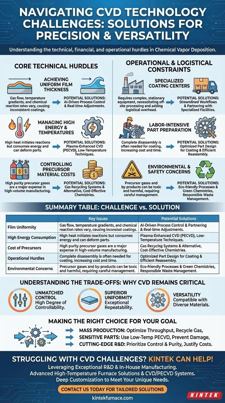
At its core, Chemical Vapor Deposition (CVD) faces four primary challenges: achieving uniform film thickness, managing high energy consumption and temperatures, controlling the high cost of precursor materials, and navigating significant operational and logistical hurdles. These challenges represent the practical constraints on a technology otherwise known for its precision and versatility in industries from semiconductors to materials science.
While CVD offers unparalleled control over thin-film properties, its industrial application is a constant balancing act. The central challenge is mitigating the high thermal, financial, and logistical costs without compromising the final material's quality and uniformity.
The Core Technical Hurdles in CVD
The fundamental physics and chemistry of the CVD process give rise to several persistent technical challenges that engineers and researchers work to overcome.
Achieving Film Uniformity at Scale
A perfectly uniform film thickness is the ideal outcome of any deposition process. However, achieving this across large or complex-shaped substrates is difficult.
Gas flow dynamics, temperature gradients, and chemical reaction rates can vary across the deposition chamber, leading to thicker or thinner coatings in different areas.
To address this, modern systems increasingly rely on AI-driven process control, which can make real-time adjustments to process parameters to ensure consistent deposition.
Managing High Temperatures and Energy Use
Traditional thermal CVD processes require extremely high temperatures to initiate the necessary chemical reactions, leading to significant energy consumption.
These high temperatures can also be destructive, causing part deformation or unwanted structural changes in the substrate material, which can degrade mechanical properties.
This has driven the development of low-temperature techniques like Plasma-Enhanced CVD (PECVD), which uses plasma to energize the precursor gases, allowing deposition to occur at much lower temperatures.
The Cost of Precursor Materials
CVD relies on highly pure, and often expensive, precursor gases. The cost of these materials can be a major factor in the overall expense of the process, especially in high-volume manufacturing.
Research is actively focused on developing alternative, more cost-effective chemistries and implementing gas recycling systems to capture and reuse unreacted precursor materials.
Navigating Operational and Logistical Constraints
Beyond the technical issues inside the reactor, implementing CVD in a production workflow presents its own set of practical challenges.
The Need for Specialized Coating Centers
CVD is not a portable technology. It requires complex, stationary equipment operating under controlled conditions, meaning it cannot be performed on-site.
This necessitates sending parts to specialized coating centers, adding significant logistical overhead, transportation costs, and lead time to the manufacturing process.
Labor-Intensive Part Preparation
For a component to be coated properly, it must often be completely disassembled. All surfaces must be exposed to the reactive gases.
This process of breaking down, coating, and reassembling parts is time-consuming and labor-intensive, adding another layer of cost and complexity.
Environmental and Safety Concerns
Many precursor gases and chemical by-products used in CVD are toxic, flammable, or environmentally harmful.
Managing these materials safely and disposing of waste responsibly is a critical challenge. This has spurred a trend toward developing more eco-friendly processes and "green" chemistries.
Understanding the Trade-offs: Why We Still Use CVD
Despite these significant challenges, CVD remains a cornerstone technology because its benefits are often impossible to achieve through other means.
Unmatched Control and Precision
The primary advantage of CVD is its high degree of controllability. Engineers can precisely adjust gas flows, pressure, and temperature to fine-tune the resulting film’s thickness, composition, and crystalline structure.
Superior Uniformity and Repeatability
When a CVD process is properly optimized, it delivers exceptional uniformity and repeatability. This consistency is non-negotiable for high-performance applications like semiconductor manufacturing, where even minor variations can lead to device failure.
Versatility Across Applications
CVD is incredibly versatile, compatible with a wide range of gases and substrate materials. It is used to create everything from silicon-based films in microchips to durable ceramic coatings on industrial tools and advanced optical layers for solar cells.
Making the Right Choice for Your Goal
Understanding these challenges allows you to strategically select and implement the right CVD approach for your specific application.
- If your primary focus is mass production: Your goal is to optimize throughput and minimize cost by exploring alternative precursors and investing in gas recycling systems.
- If your primary focus is coating sensitive or complex parts: Low-temperature processes like PECVD are necessary to prevent thermal damage and deformation of the underlying substrate.
- If your primary focus is cutting-edge R&D: The priority is process control and material purity, where the higher costs of advanced precursors and equipment are justified by the pursuit of novel properties.
Recognizing these inherent challenges is the first step toward successfully leveraging the immense power and precision of CVD technology.
Summary Table:
| Challenge | Key Issues | Potential Solutions |
|---|---|---|
| Film Uniformity | Gas flow variations, temperature gradients | AI-driven process control, optimized chamber design |
| High Energy Consumption | High temperatures, part deformation | Use of Plasma-Enhanced CVD (PECVD), low-temperature techniques |
| Cost of Precursors | Expensive gases, material purity | Gas recycling systems, alternative chemistries |
| Operational Hurdles | Logistical issues, labor-intensive prep | Specialized coating centers, streamlined workflows |
| Environmental Concerns | Toxic by-products, safety risks | Eco-friendly processes, green chemistries |
Struggling with CVD challenges in your lab? KINTEK can help! Leveraging exceptional R&D and in-house manufacturing, we provide advanced high-temperature furnace solutions like Muffle, Tube, Rotary Furnaces, Vacuum & Atmosphere Furnaces, and CVD/PECVD Systems. Our strong deep customization capability ensures we precisely meet your unique experimental needs, enhancing efficiency and overcoming hurdles like film uniformity and high costs. Contact us today to discuss how our tailored solutions can optimize your CVD processes!
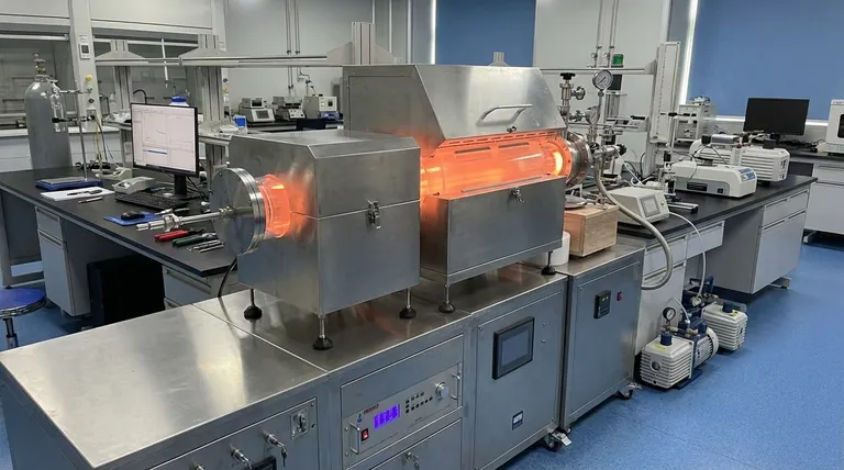
Visual Guide
Related Products
- Custom Made Versatile CVD Tube Furnace Chemical Vapor Deposition CVD Equipment Machine
- Multi Heating Zones CVD Tube Furnace Machine for Chemical Vapor Deposition Equipment
- HFCVD Machine System Equipment for Drawing Die Nano Diamond Coating
- Split Chamber CVD Tube Furnace with Vacuum Station CVD Machine
- 915MHz MPCVD Diamond Machine Microwave Plasma Chemical Vapor Deposition System Reactor
People Also Ask
- What is a CVD tube furnace and what is its primary function? Discover Precision Thin-Film Deposition
- Why are CVD tube furnace sintering systems indispensable for 2D material research and production? Unlock Atomic-Scale Precision
- How might AI and machine learning enhance CVD tube furnace processes? Boost Quality, Speed, and Safety
- What is the working principle of a CVD tube furnace? Achieve Precise Thin Film Deposition for Your Lab
- What improvements can be made to the bonding force of gate dielectric films using a CVD tube furnace? Enhance Adhesion for Reliable Devices


