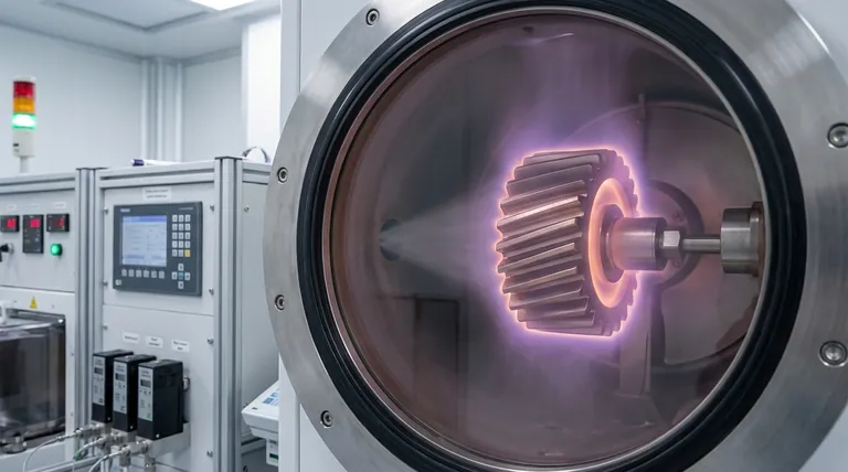
At its core, Chemical Vapor Deposition (CVD) is a process uniquely capable of producing exceptionally pure, uniform, and conformal films. Its primary advantages stem from its use of gaseous chemical precursors, which allows for the precise deposition of materials onto substrates of virtually any shape, enabling the creation of high-performance coatings and advanced electronic components.
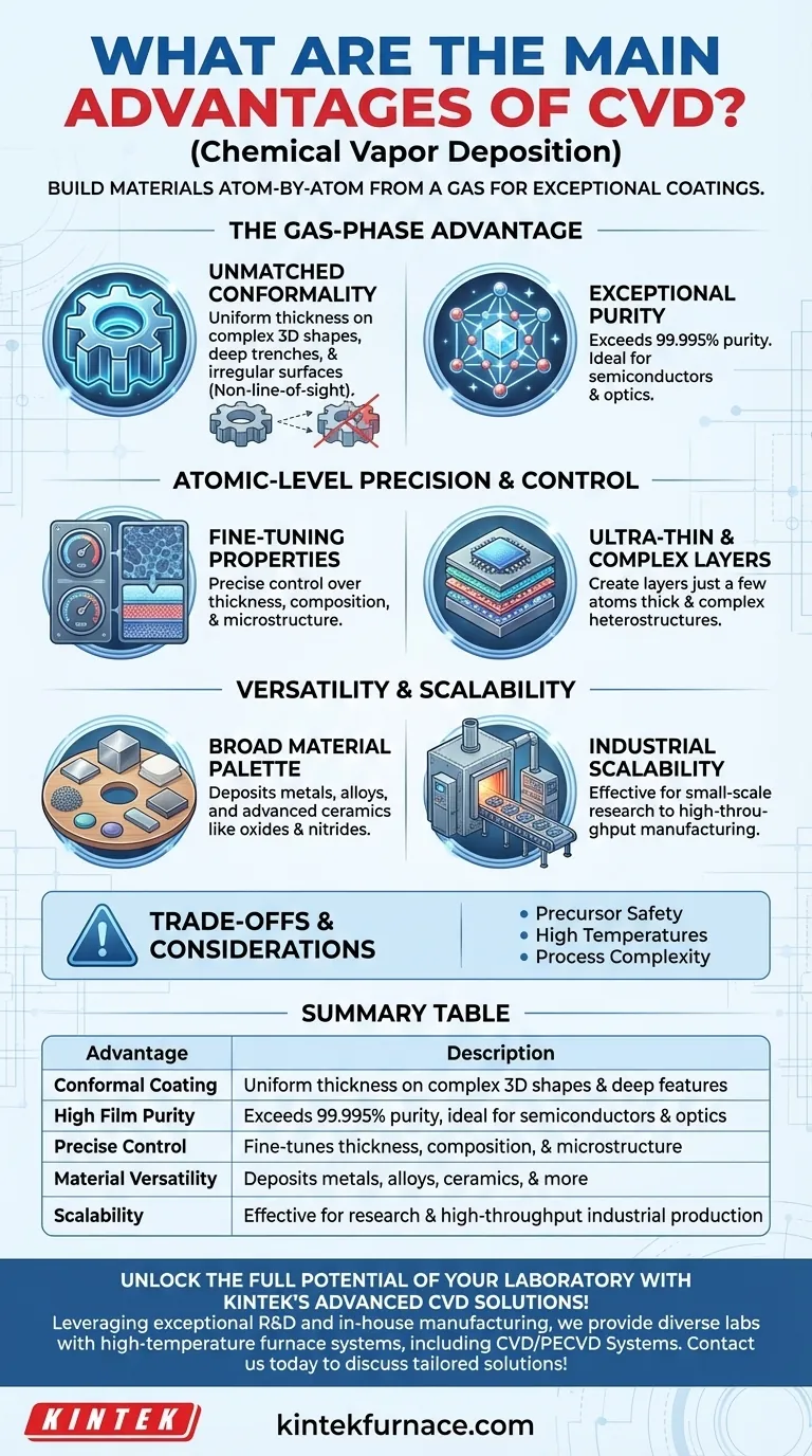
While many techniques can apply a coating, CVD's fundamental advantage is its ability to build materials atom-by-atom from a gas. This allows it to create flawless, uniform layers on even the most intricate three-dimensional surfaces, a feat that physical, line-of-sight methods cannot easily replicate.
The Foundational Advantage: The Gas-Phase Approach
The defining characteristic of CVD is that the coating material is delivered in a gaseous state. This simple principle is the source of its most powerful benefits.
Unmatched Conformality and Uniformity
Because the reactants are gases, they flow and diffuse to cover every exposed area of a substrate. This results in a highly conformal coating that maintains a uniform thickness, even inside deep trenches, around sharp corners, or on complex, irregular shapes.
This non-line-of-sight capability is a significant advantage over physical vapor deposition (PVD) methods, which struggle to coat surfaces not directly facing the material source.
Exceptional Film Purity
CVD precursors can be refined to extremely high levels of purity before they enter the reaction chamber. The process itself is also largely self-cleaning.
As a result, the deposited films can achieve purity levels exceeding 99.995%, a critical requirement for high-performance applications in the semiconductor and optical industries.
Precision and Control at the Atomic Level
CVD offers a degree of control that is essential for engineering modern, high-tech materials and devices.
Fine-Tuning Film Properties
By precisely managing process parameters like temperature, pressure, and the flow rates of different precursor gases, operators can meticulously control the final film.
This allows for the fine-tuning of a material's thickness, composition, and microstructure, such as grain size and crystal orientation, to meet exact specifications.
Creating Ultra-Thin and Complex Layers
This precise control enables the deposition of ultra-thin films, sometimes just a few atomic layers thick.
It also makes CVD ideal for creating complex, multi-layered structures (heterostructures) by simply changing the precursor gases during the process, a cornerstone of modern microelectronics and nanotechnology.
Versatility for Diverse Applications
CVD is not a single process but a family of techniques adaptable to a vast range of materials and industries.
A Broad Palette of Materials
One of CVD's most significant advantages is its versatility. By selecting the appropriate precursor chemistry, it can be used to deposit a wide variety of materials.
This includes metals, alloys, and advanced ceramics like oxides and nitrides. This flexibility makes it invaluable across industries from aerospace to biomedical devices.
Scalability for Industrial Production
The process is highly scalable, proven effective for both small-scale research and high-throughput industrial manufacturing. It can be adapted to coat large-area substrates, like architectural glass, or to process many smaller parts simultaneously in a batch reactor.
Understanding the Trade-offs
No process is perfect. While powerful, the advantages of CVD come with practical considerations.
Precursor Chemistry and Safety
The chemical precursors used in CVD are often highly toxic, flammable, or corrosive. This necessitates sophisticated handling protocols, delivery systems, and safety equipment, which can increase operational complexity and cost.
High Temperature Requirements
Traditional CVD processes often operate at very high temperatures. While this can improve film quality and adhesion, it makes the process unsuitable for temperature-sensitive substrates like polymers or certain electronic components. Low-temperature variants (e.g., PECVD) exist to mitigate this, but they may involve their own compromises.
Process Complexity
Developing a stable, repeatable CVD recipe for a specific material on a specific substrate is a complex task. It requires significant expertise in chemistry and materials science to optimize the many interdependent process variables.
Making the Right Choice for Your Application
Selecting CVD depends entirely on your end goal and technical requirements.
- If your primary focus is coating complex 3D parts or deep features: CVD's exceptional conformality is its standout feature, ensuring uniform coverage where line-of-sight methods would fail.
- If your primary focus is extreme material purity for electronics or optics: CVD's use of purified gaseous precursors delivers films with purity levels that are difficult to achieve otherwise.
- If your primary focus is creating advanced nanostructures or multi-layer devices: CVD's precise control over thickness and composition allows for atomic-level engineering of materials.
- If your primary focus is scalable production of durable, high-performance coatings: CVD is a proven, cost-effective choice for many industrial applications once the process is optimized.
Ultimately, the advantages of CVD make it an indispensable tool for engineering materials from the atom up, enabling technologies that would otherwise be impossible.
Summary Table:
| Advantage | Description |
|---|---|
| Conformal Coating | Uniform thickness on complex 3D shapes and deep features |
| High Film Purity | Exceeds 99.995% purity, ideal for semiconductors and optics |
| Precise Control | Fine-tunes thickness, composition, and microstructure |
| Material Versatility | Deposits metals, alloys, ceramics, and more |
| Scalability | Effective for research and high-throughput industrial production |
Unlock the full potential of your laboratory with KINTEK's advanced CVD solutions! Leveraging exceptional R&D and in-house manufacturing, we provide diverse labs with high-temperature furnace systems, including CVD/PECVD Systems, Muffle, Tube, Rotary, Vacuum & Atmosphere Furnaces. Our strong deep customization capability ensures we precisely meet your unique experimental needs for superior film deposition. Contact us today to discuss how our tailored solutions can enhance your research and production efficiency!
Visual Guide
Related Products
- Custom Made Versatile CVD Tube Furnace Chemical Vapor Deposition CVD Equipment Machine
- Multi Heating Zones CVD Tube Furnace Machine for Chemical Vapor Deposition Equipment
- HFCVD Machine System Equipment for Drawing Die Nano Diamond Coating
- Split Chamber CVD Tube Furnace with Vacuum Station CVD Machine
- 915MHz MPCVD Diamond Machine Microwave Plasma Chemical Vapor Deposition System Reactor
People Also Ask
- Which industries and research fields benefit from CVD tube furnace sintering systems for 2D materials? Unlock Next-Gen Tech Innovations
- What is a CVD tube furnace and what is its primary function? Discover Precision Thin-Film Deposition
- What are the key features of CVD tube furnaces for 2D material processing? Unlock Precision Synthesis for Superior Materials
- What are the key application fields of CVD tube furnaces? Unlock Precision in Thin-Film Synthesis
- How might AI and machine learning enhance CVD tube furnace processes? Boost Quality, Speed, and Safety


