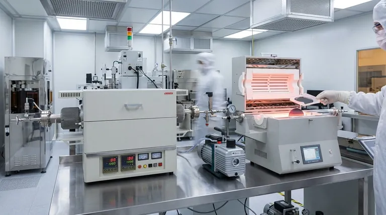
In the semiconductor and optoelectronics industries, vacuum tube furnaces are primarily used for mission-critical thermal processes like chemical vapor deposition (CVD), annealing, and sintering. These processes require an ultra-clean, controlled environment to create the high-purity, defect-free materials that form the foundation of integrated circuits, sensors, and optical devices. The vacuum prevents unwanted chemical reactions, chiefly oxidation, that would otherwise compromise device performance and reliability.
The fundamental role of a vacuum furnace is not just to heat materials, but to do so in an environment free from atmospheric contaminants. This control is the key to fabricating semiconductor and optoelectronic components with the precise electrical and optical properties required for modern technology.
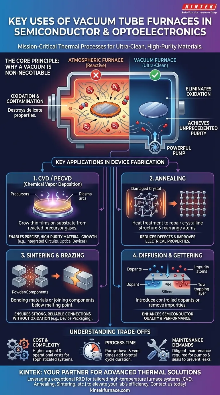
The Core Principle: Why a Vacuum is Non-Negotiable
At the high temperatures used in semiconductor manufacturing, materials become highly reactive. A standard furnace, which heats in the presence of air, would instantly destroy the delicate properties of a silicon wafer. A vacuum furnace removes this threat.
Eliminating Oxidation and Contamination
The primary purpose of the vacuum is to remove reactive gases, especially oxygen. At elevated temperatures, oxygen readily bonds with silicon and other materials, forming unwanted oxide layers that can ruin a device's electrical characteristics.
By operating at pressures far below atmospheric levels, the furnace chamber is virtually free of contaminants, ensuring that the only chemical reactions that occur are the ones you intentionally introduce.
Achieving Unprecedented Material Purity
Semiconductor devices rely on materials with impurity levels measured in parts per billion. Even trace amounts of an unintended element can dramatically alter a material's conductivity and render a microchip useless.
A vacuum environment is the first line of defense in maintaining this ultra-high purity throughout the manufacturing process.
Enabling Precise Chemical Processes
Many critical processes involve introducing specific gases into the chamber to build or modify materials. A vacuum ensures the chamber is a blank slate before these precursor gases are introduced.
This allows processes like Chemical Vapor Deposition (CVD) to proceed with absolute precision, as only the intended gases are present to react and form a thin film on the wafer's surface.
Key Applications in Device Fabrication
The controlled environment of a vacuum furnace is leveraged for several distinct, critical manufacturing steps.
Chemical Vapor Deposition (CVD and PECVD)
CVD is a process used to grow thin films of material on a substrate. In a vacuum furnace, precursor gases are introduced and react on the hot wafer surface, depositing a solid layer.
This method is essential for creating the silicon, metal, and inorganic films that form the complex, layered structures of integrated circuits and optoelectronic devices. Plasma-Enhanced CVD (PECVD) is a variation that uses plasma to allow deposition at lower temperatures.
Annealing
Annealing is a heat treatment process used to repair and improve a material's crystalline structure. During fabrication, processes like ion implantation can damage the silicon crystal lattice.
Heating the wafer in a vacuum furnace allows the atoms to rearrange themselves back into a near-perfect structure, reducing defects and improving the material's electrical properties. The vacuum is critical to prevent the wafer from oxidizing during this high-temperature step.
Sintering and Brazing
Sintering involves heating compacted material powders below their melting point to bond the particles together, forming a solid, dense structure. Brazing uses a filler metal to join two components together.
In electronics, these processes are used for creating robust device packaging and contacts. Performing them in a vacuum prevents the formation of weak, oxidized layers at the joints, ensuring strong, reliable connections.
Diffusion and Gettering
A vacuum furnace provides the ideal environment for diffusion, the process of intentionally introducing controlled impurities (dopants) into the silicon wafer to create P-type and N-type regions.
It is also used for gettering, a process that uses heat to actively draw out and trap unwanted impurities from the active areas of the wafer, further enhancing its quality and performance.
Understanding the Trade-offs
While indispensable, vacuum furnaces present unique challenges compared to atmospheric heating systems.
Cost and Complexity
Vacuum systems are inherently more complex and expensive to build and operate. They require sophisticated pumps, seals, and monitoring gauges to achieve and maintain low pressures, adding significant capital and operational cost.
Process Time and Throughput
Achieving a high vacuum is not instantaneous. The time required to pump down the chamber before processing and vent it afterward adds to the total cycle time for each batch of wafers. This can limit factory throughput compared to continuous, atmospheric processes.
Maintenance Demands
The components of a vacuum system, particularly pumps and seals, are subject to wear and require diligent, preventative maintenance. Failure to maintain the system can lead to leaks, contamination, and costly production failures.
Making the Right Choice for Your Goal
Selecting the correct thermal process is determined by the specific outcome you need to achieve.
- If your primary focus is building high-purity thin films: CVD or PECVD inside a vacuum furnace is the industry standard for precise control over film composition and quality.
- If your primary focus is repairing crystal damage and boosting electrical performance: Vacuum annealing is the only way to heat a wafer without introducing new, performance-killing defects from oxidation.
- If your primary focus is joining components with maximum strength and electrical integrity: Vacuum brazing or sintering is essential to prevent weak oxide layers from forming at the joint interface.
- If your primary focus is controlling the dopant profile of a semiconductor: Diffusion in a controlled vacuum environment provides the precision needed to create reliable electronic junctions.
Ultimately, mastering vacuum-based thermal processing is fundamental to fabricating the high-performance devices that power our modern world.
Summary Table:
| Process | Key Use in Industries | Benefit |
|---|---|---|
| CVD / PECVD | Thin film deposition for integrated circuits and optical devices | Enables precise, high-purity material growth |
| Annealing | Repairs crystal damage in silicon wafers | Reduces defects and improves electrical properties |
| Sintering / Brazing | Joins components for robust packaging and contacts | Ensures strong, reliable connections without oxidation |
| Diffusion / Gettering | Introduces dopants and removes impurities | Enhances semiconductor quality and performance |
Ready to elevate your semiconductor and optoelectronics manufacturing with advanced vacuum tube furnaces? KINTEK leverages exceptional R&D and in-house manufacturing to provide high-temperature furnace solutions tailored to your needs. Our product line includes Muffle, Tube, Rotary Furnaces, Vacuum & Atmosphere Furnaces, and CVD/PECVD Systems, all backed by strong deep customization capabilities to precisely meet your unique experimental requirements. Contact us today to discuss how we can enhance your lab's efficiency and device performance!
Visual Guide
Related Products
- Vacuum Hot Press Furnace Machine Heated Vacuum Press Tube Furnace
- Vacuum Sealed Continuous Working Rotary Tube Furnace Rotating Tube Furnace
- High Pressure Laboratory Vacuum Tube Furnace Quartz Tubular Furnace
- Laboratory Vacuum Tilt Rotary Tube Furnace Rotating Tube Furnace
- Magnesium Extraction and Purification Condensing Tube Furnace
People Also Ask
- What safety features are incorporated in vacuum hot press furnaces? Ensure Operator and Equipment Protection
- What temperature control features do vacuum hot press furnaces have? Achieve Precision in High-Temp Material Processing
- What are the benefits of the vacuum environment system in a vacuum hot press furnace? Unlock High-Density Sintering
- What control features does a vacuum hot press furnace offer? Precision Control for Advanced Materials Processing
- Why use Vacuum Hot Press (VHP) for ZnS Ceramics? Achieve Superior IR Transparency and Mechanical Strength


