At their core, inductive discharges offer two primary advantages in Plasma-Enhanced Chemical Vapor Deposition (PECVD): significantly higher deposition rates and independent control over the energy of ions bombarding the substrate. This is achieved by generating a much denser plasma than conventional methods, which more efficiently breaks down precursor gases into the building blocks needed for film growth.
The fundamental advantage of an inductive discharge is not just higher density, but its ability to decouple plasma generation from substrate biasing. This allows you to independently control deposition rate (via plasma density) and film properties like stress and damage (via ion energy), a level of control that is impossible in simpler capacitive systems.
The Core Principle: Decoupling Power from Ion Energy
To understand the benefits of inductive discharges, we must first contrast them with their more common counterpart, the capacitive discharge.
How Capacitive Plasmas Work (The Baseline)
In a standard PECVD system, a single radio frequency (RF) power source is applied to one of the electrodes, creating a capacitively coupled plasma (CCP). This single power source is responsible for both creating the plasma and accelerating ions toward the substrate.
The two functions are inextricably linked. If you increase the power to create a denser plasma for faster deposition, you also inevitably increase the energy of the ions hitting your film, which can cause damage, increase stress, and alter film properties.
How Inductive Plasmas Work (The Advantage)
An inductively coupled plasma (ICP) uses a different method. An RF current is passed through a coil, which induces a powerful electromagnetic field inside the chamber. This field efficiently energizes and accelerates electrons within the bulk of the plasma itself, not just at the edges.
This creates an extremely dense plasma. Crucially, a separate, lower-power RF source can be applied to the substrate holder to independently control the ion energy. This "decoupling" gives the process engineer two separate knobs: one for plasma density (the ICP coil) and one for ion energy (the substrate bias).
Key Advantages of Inductive Discharges
This fundamental difference in operation leads to several distinct, practical advantages for materials processing.
Higher Plasma Density and Deposition Rates
Because the inductive coil is so efficient at transferring energy to the plasma, it can sustain densities that are 100 to 1000 times higher than a typical capacitive discharge.
More plasma density means more reactive chemical species are generated from the precursor gases. This massive increase in available reactants directly translates to significantly faster film deposition rates, increasing wafer throughput in a manufacturing environment.
Enhanced Precursor Dissociation
The high-density, high-energy electrons in an inductive discharge are extremely effective at breaking down precursor gas molecules. This complete dissociation is critical for forming high-purity films.
Incomplete dissociation can leave unwanted atoms (like hydrogen in silicon nitride films) or molecular fragments incorporated into the film, which can degrade its electrical or mechanical properties. The efficiency of an ICP source minimizes these impurities.
Low (and Controllable) Ion Bombardment
Perhaps the most sophisticated advantage is the ability to combine high deposition rates with low-energy ion bombardment. Because ion energy is controlled by the separate substrate bias, you can turn it down to very low levels.
This is critical for depositing high-quality films on sensitive substrates that could be damaged by high-energy ions. It also allows for the growth of films with very low intrinsic stress, which is essential for applications in MEMS and advanced optics.
Understanding the Trade-offs
No technology is without its compromises. While powerful, inductive discharges come with their own set of challenges.
System Complexity and Cost
ICP-PECVD reactors are inherently more complex than their CCP counterparts. They require a second RF power supply, a sophisticated matching network for the coil, and careful engineering of the coil and its dielectric window, making them significantly more expensive to purchase and maintain.
Plasma Uniformity Challenges
Achieving a highly uniform plasma over a very large substrate (e.g., 300mm wafers or large-area glass) can be challenging with an inductive coil design. It requires meticulous engineering of the coil geometry and chamber to prevent "hot spots" in the plasma that would lead to non-uniform film thickness.
Making the Right Choice for Your Goal
The choice between an inductive and a capacitive discharge depends entirely on the technical requirements and economic constraints of your application.
- If your primary focus is high throughput and speed: Inductive discharge is the clear choice due to its ability to generate high-density plasmas and achieve superior deposition rates.
- If your primary focus is high-quality films on sensitive substrates: The decoupled nature of inductive discharges offers unmatched control, enabling low-damage, low-stress deposition that is impossible with CCP.
- If your primary focus is cost-effectiveness for less demanding applications: A traditional capacitive discharge (CCP) system remains a robust, reliable, and more economical solution for many standard deposition needs.
Ultimately, understanding the physics of how your plasma is generated is the first step toward mastering your deposition process and achieving the desired film properties.
Summary Table:
| Advantage | Description |
|---|---|
| Higher Deposition Rates | Achieves up to 100-1000x faster deposition due to dense plasma generation. |
| Independent Ion Energy Control | Allows separate adjustment of plasma density and ion energy for low-damage films. |
| Enhanced Precursor Dissociation | Improves film purity by efficiently breaking down gas molecules. |
| Low Ion Bombardment | Protects sensitive substrates and reduces film stress in applications like MEMS and optics. |
Unlock the full potential of your lab with KINTEK's advanced high-temperature furnace solutions! Leveraging exceptional R&D and in-house manufacturing, we provide diverse laboratories with cutting-edge PECVD systems, including our CVD/PECVD line, designed to deliver high deposition rates and precise control for sensitive substrates. Our strong deep customization capability ensures we can tailor solutions to meet your unique experimental needs. Contact us today to discuss how we can enhance your materials processing efficiency and film quality!
Visual Guide

Related Products
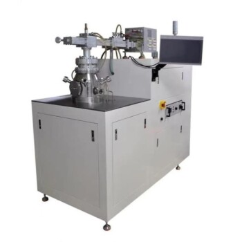
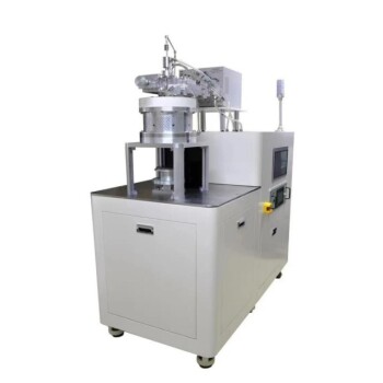
- RF PECVD System Radio Frequency Plasma Enhanced Chemical Vapor Deposition
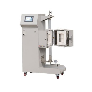
- Inclined Rotary Plasma Enhanced Chemical Deposition PECVD Tube Furnace Machine
- Inclined Rotary Plasma Enhanced Chemical Deposition PECVD Tube Furnace Machine
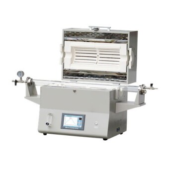
- Custom Made Versatile CVD Tube Furnace Chemical Vapor Deposition CVD Equipment Machine
- HFCVD Machine System Equipment for Drawing Die Nano Diamond Coating
People Also Ask
- What is PECVD equipment? A Guide to Low-Temperature Thin-Film Deposition
- What is plasma enhanced chemical vapor deposition application? Enable High-Performance Thin Films at Lower Temperatures
- What is the second benefit of deposition within a discharge in PECVD? Enhance Film Quality with Ion Bombardment
- What information does laboratory XRD provide for Gallium Sulfide? Master GaS Single Crystal Characterization
- How does plasma enhanced CVD work? Achieve Low-Temperature, High-Quality Thin Film Deposition

