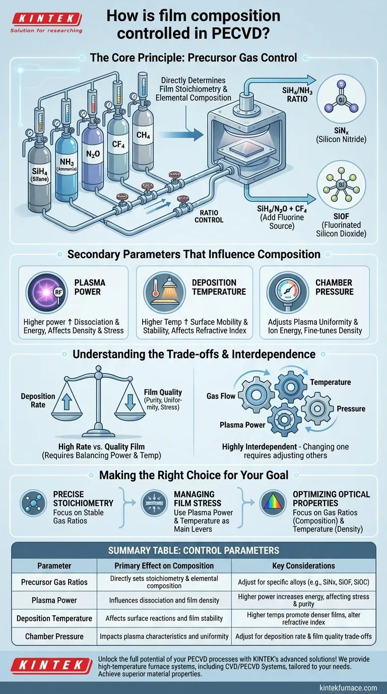
In short, film composition in PECVD is controlled by precisely managing the flow rates and ratios of the precursor gases introduced into the deposition chamber. By adjusting the mix of these gases, you directly determine which chemical elements are available to form the thin film, allowing you to create materials with specific stoichiometries and properties.
While precursor gas ratios are the primary control for chemical composition, achieving a high-quality, functional film requires a holistic approach. The true art of PECVD lies in balancing gas flows with secondary parameters like plasma power and temperature, as each variable influences the others.
The Core Principle: Precursor Gas Control
The fundamental job of PECVD is to break down gaseous molecules (precursors) and deposit them as a solid film. The composition of that film is a direct result of the building blocks you provide.
The Role of Gas Flow Rates and Ratios
The ratio of different precursor gases is the most direct lever you can pull to control stoichiometry, which is the quantitative relationship between elements in a compound.
For example, when depositing silicon nitride (SiNx), the ratio of a silicon-containing gas (like silane, SiH4) to a nitrogen-containing gas (like ammonia, NH3) will determine the final Si-to-N ratio in the film. This, in turn, heavily influences the film's electrical and mechanical properties.
Introducing New Elements for Tuned Properties
Beyond basic stoichiometry, you can introduce additional gases to intentionally incorporate new elements and create advanced alloys.
This technique expands the range of achievable film properties. Adding a fluorine-containing gas can produce fluorinated silicon dioxide (SiOF), which has a lower dielectric constant. Similarly, introducing a carbon source can yield silicon oxycarbide (SiOC), a hard and chemically resistant material.
Secondary Parameters That Influence Composition
While gas flow sets the available ingredients, other process parameters determine how those ingredients react and incorporate into the film. They are critical for fine-tuning properties like density, purity, and stress.
Plasma Power
The RF power applied to create the plasma determines the energy available to break down the precursor gas molecules.
Higher power can lead to more complete dissociation of gases, potentially altering which species are incorporated into the film. It's a key parameter for controlling film density and managing internal stress.
Deposition Temperature
Substrate temperature influences the surface mobility of the deposited atoms and the rate of surface chemical reactions.
A higher temperature can promote denser, more stable films by giving atoms more energy to find their ideal place in the crystal or amorphous structure. This can subtly affect the final composition and significantly impact properties like the refractive index.
Chamber Pressure
Operating pressure affects the mean free path of particles and the characteristics of the plasma.
Adjusting pressure can influence the uniformity of the deposition and the energy with which ions strike the surface, providing another way to fine-tune film density and composition.
Understanding the Trade-offs
Controlling film composition is not as simple as setting a gas ratio. Each parameter adjustment comes with consequences that must be managed.
Deposition Rate vs. Film Quality
Increasing gas flow rates will generally increase the deposition rate, allowing you to grow thicker films faster.
However, a very high deposition rate can lead to lower-quality films with higher impurity levels, poor uniformity, or unfavorable stress. The process must provide enough energy (via plasma and temperature) to properly react the supplied gases.
The Interdependence of Variables
The parameters in a PECVD process are highly interdependent. Changing one will almost always require you to adjust others to maintain the desired outcome.
For instance, increasing the gas flow might require a corresponding increase in plasma power to ensure the gases are fully dissociated. Failing to balance these factors can lead to unwanted chemical reactions or a film composition that deviates from your target.
Making the Right Choice for Your Goal
Your process recipe should be guided by your primary objective for the film.
- If your primary focus is precise stoichiometry: Begin by establishing stable, repeatable gas flow ratios as your baseline.
- If your primary focus is managing film stress: Use plasma power and temperature as your main levers for tuning, while making only minor adjustments to gas flow.
- If your primary focus is optimizing optical properties: Focus on the interplay between gas ratios (for composition) and temperature (for density) to control the refractive index.
Ultimately, mastering film composition in PECVD is about understanding and controlling a multi-variable system to achieve a specific material property.
Summary Table:
| Control Parameter | Primary Effect on Film Composition | Key Considerations |
|---|---|---|
| Precursor Gas Ratios | Directly sets stoichiometry and elemental composition | Adjust SiH4/NH3 for SiNx; add gases for alloys like SiOF or SiOC |
| Plasma Power | Influences dissociation and film density | Higher power increases energy, affecting stress and purity |
| Deposition Temperature | Affects surface reactions and film stability | Higher temps promote denser films and alter refractive index |
| Chamber Pressure | Impacts plasma characteristics and uniformity | Adjust for deposition rate and film quality trade-offs |
Unlock the full potential of your PECVD processes with KINTEK's advanced solutions! Leveraging our exceptional R&D and in-house manufacturing, we provide diverse laboratories with high-temperature furnace systems, including CVD/PECVD Systems, tailored to your unique experimental needs. Our deep customization capabilities ensure precise control over film composition, helping you achieve superior material properties in semiconductors, optics, and beyond. Contact us today to discuss how we can enhance your deposition outcomes and drive innovation in your research or production!
Visual Guide
Related Products
- Slide PECVD Tube Furnace with Liquid Gasifier PECVD Machine
- RF PECVD System Radio Frequency Plasma Enhanced Chemical Vapor Deposition
- Inclined Rotary Plasma Enhanced Chemical Deposition PECVD Tube Furnace Machine
- Inclined Rotary Plasma Enhanced Chemical Deposition PECVD Tube Furnace Machine
- Multi Heating Zones CVD Tube Furnace Machine for Chemical Vapor Deposition Equipment
People Also Ask
- In which industries is the tube furnace commonly used? Essential for Materials Science, Energy, and More
- What role does a Tube Furnace play in the CVD growth of carbon nanotubes? Achieve High-Purity CNT Synthesis
- What plasma source is used in PE-CVD tube furnaces? Unlock Low-Temperature, High-Quality Deposition
- What is plasma in the context of PECVD? Unlock Low-Temperature Thin Film Deposition
- What are the disadvantages of tube furnace cracking when processing heavy raw materials? Avoid Costly Downtime and Inefficiency


