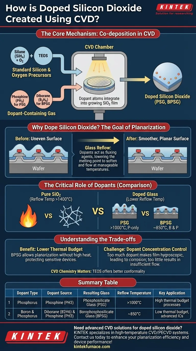
Doped silicon dioxide is created during a Chemical Vapor Deposition (CVD) process by introducing a dopant-containing gas alongside the standard silicon and oxygen precursor gases. For example, phosphine (PH3) is used to add phosphorus, and a boron source like diborane (B2H6) is used to add boron. These dopant atoms become integrated into the silicon dioxide film as it grows on the wafer, forming a doped glass.
The central purpose of doping silicon dioxide is not to alter its electrical properties, but to fundamentally change its physical behavior. By adding impurities like phosphorus and boron, you significantly lower the glass's melting point, enabling it to soften and "flow" at manageable temperatures to create a smoother, more planar surface.
The Core Mechanism: Co-deposition in CVD
The creation of doped oxide is a modification of a standard silicon dioxide deposition process. The key is the simultaneous introduction of all necessary chemical precursors in the gas phase.
Starting with a Standard SiO2 Process
In a typical CVD process, a silicon source gas is reacted with an oxygen source to form solid silicon dioxide (SiO2) on the wafer's surface. Common chemistries include:
- Silane (SiH4) and Oxygen (O2), typically at lower temperatures (300-500°C).
- Tetraethylorthosilicate (TEOS), which thermally decomposes at higher temperatures (650-750°C) to form high-quality SiO2.
Introducing the Dopant Source
To create a doped film, a third gas containing the desired impurity is added to the gas mixture flowing into the CVD chamber.
- To create phosphorus-doped glass (PSG), phosphine (PH3) gas is used.
- To create borophosphosilicate glass (BPSG), both phosphine and a boron source like diborane (B2H6) are introduced.
Incorporation into the Growing Film
As the chemical reaction proceeds and the SiO2 film deposits atom by atom, the dopant atoms are incorporated directly into the glass structure. They substitute some of the silicon or oxygen atoms, disrupting the pure SiO2 network and changing its physical properties.
Why Dope Silicon Dioxide? The Goal of Planarization
The primary driver for doping oxide films in semiconductor manufacturing is to solve the challenge of device topography.
The Problem: Uneven Surfaces
As transistors and wires are built on a wafer, they create a surface with significant "hills and valleys." Depositing a subsequent insulating layer over this uneven topography results in a conformal film that replicates the bumps, which is detrimental to the photolithography and metal interconnects that come next.
The Solution: Glass Reflow
The solution is to deposit a glass layer and then heat the wafer until the glass softens, much like honey. The force of surface tension causes the semi-liquid glass to flow, filling the valleys and rounding the sharp corners to create a much smoother, more planar surface.
The Critical Role of Dopants
Pure SiO2 has an extremely high softening point (well above 1400°C), a temperature that would destroy the delicate transistors already on the wafer. Dopants act as fluxing agents, breaking up the rigid SiO2 atomic network and dramatically lowering the temperature at which the glass reflows.
- Phosphosilicate Glass (PSG), also known as P-glass, is doped only with phosphorus. It requires temperatures above 1000°C to flow effectively.
- Borophosphosilicate Glass (BPSG) is doped with both boron and phosphorus. The combination of dopants lowers the reflow temperature even further, to around 850°C.
Understanding the Trade-offs
While essential, using doped oxides introduces process complexities that must be carefully managed.
The Benefit: A Lower Thermal Budget
The single greatest advantage of BPSG over PSG is its lower reflow temperature. This is critical in modern manufacturing, as it allows for planarization without exposing underlying sensitive structures to damagingly high heat.
The Challenge: Dopant Concentration Control
The percentage of dopants in the glass is a critical parameter. Too little dopant, and the glass won't flow sufficiently at the target temperature. Too much dopant can make the film unstable and hygroscopic, meaning it readily absorbs moisture from the air, which can lead to the formation of acids that corrode metal wiring.
The Impact of CVD Chemistry
The choice of base SiO2 chemistry (e.g., Silane vs. TEOS) still matters. TEOS-based oxides typically provide better conformality, meaning the film is more uniform in thickness over sharp steps before the reflow step. This results in a more uniform final planarized surface.
Making the Right Choice for Your Process
Your decision depends almost entirely on the thermal constraints of your overall manufacturing flow.
- If your primary focus is simplicity with a high thermal budget (>1000°C): PSG is a well-understood and effective option for planarization in processes that can tolerate high temperatures.
- If your primary focus is protecting temperature-sensitive devices (<900°C): BPSG is the essential choice, providing excellent planarization at the lower temperatures required for advanced integrated circuits.
- If your primary focus is simple electrical isolation without planarization: An undoped oxide from a TEOS or silane source is simpler and avoids the complexities of dopant control.
Understanding how dopants modify glass flow is fundamental to achieving the precise surface topography required for reliable, high-performance device fabrication.
Summary Table:
| Dopant Type | Dopant Source | Resulting Glass | Reflow Temperature | Key Application |
|---|---|---|---|---|
| Phosphorus | Phosphine (PH3) | Phosphosilicate Glass (PSG) | >1000°C | High thermal budget processes |
| Boron & Phosphorus | Diborane (B2H6) & Phosphine (PH3) | Borophosphosilicate Glass (BPSG) | ~850°C | Low thermal budget, advanced ICs |
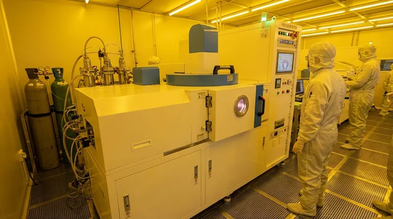
Need advanced CVD solutions for doped silicon dioxide? KINTEK specializes in high-temperature furnace systems, including CVD/PECVD models, tailored for semiconductor labs. With our deep customization and in-house manufacturing, we ensure precise control for processes like PSG and BPSG deposition. Contact us today to enhance your planarization efficiency and device performance!
Visual Guide
Related Products
- Custom Made Versatile CVD Tube Furnace Chemical Vapor Deposition CVD Equipment Machine
- Inclined Rotary Plasma Enhanced Chemical Deposition PECVD Tube Furnace Machine
- Inclined Rotary Plasma Enhanced Chemical Deposition PECVD Tube Furnace Machine
- Slide PECVD Tube Furnace with Liquid Gasifier PECVD Machine
- Multi Heating Zones CVD Tube Furnace Machine for Chemical Vapor Deposition Equipment
People Also Ask
- Why are CVD tube furnace sintering systems indispensable for 2D material research and production? Unlock Atomic-Scale Precision
- How does CVD tube furnace sintering enhance graphene growth? Achieve Superior Crystallinity and High Electron Mobility
- Which industries and research fields benefit from CVD tube furnace sintering systems for 2D materials? Unlock Next-Gen Tech Innovations
- What future trends are expected in the development of CVD tube furnaces? Discover Smarter, More Versatile Systems
- What customization options are available for CVD tube furnaces? Tailor Your System for Superior Material Synthesis


