In solar cell manufacturing, Chemical Vapor Deposition (CVD) is the foundational technique used to construct the critical, ultra-thin functional layers of a photovoltaic device. It precisely deposits materials—from the primary light-absorbing layer to performance-enhancing coatings—onto a substrate. This atomic-level control over film thickness and composition is essential for optimizing the cell's efficiency and cost-effectiveness.
CVD and its variants are indispensable for modern solar cells because they allow for the precise construction of thin films. This control directly translates to higher sunlight absorption, improved electron flow, and ultimately, greater energy conversion efficiency and durability.
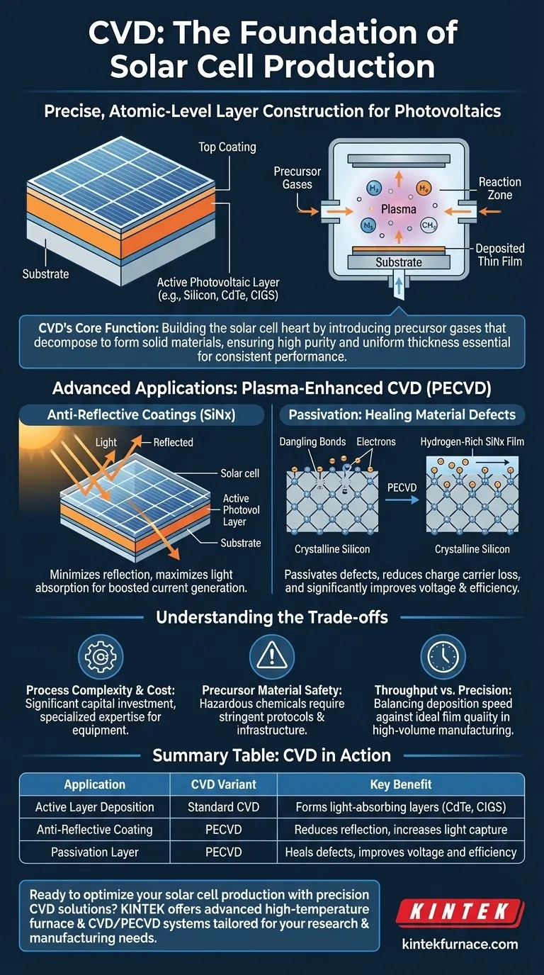
The Core Function: Building a Solar Cell Layer by Layer
The primary role of CVD in this context is to build the functional heart of the solar cell. It achieves this by introducing precursor gases into a reaction chamber, which then decompose and deposit a solid material onto the solar cell substrate.
Depositing the Active Photovoltaic Layer
For many thin-film solar cells, CVD is the process used to create the very layer that absorbs sunlight and converts it into electricity.
This active layer can be made of various photovoltaic materials, including silicon, cadmium telluride (CdTe), or copper indium gallium selenide (CIGS).
Achieving High Purity and Uniformity
The CVD process allows for exceptionally precise control over the deposition rate. This ensures the resulting film has a highly uniform thickness and purity across the entire substrate.
This uniformity is critical for consistent and predictable performance, as variations in thickness or impurities can severely degrade a solar cell's efficiency.
Advanced Applications: Plasma-Enhanced CVD (PECVD)
A specific and widely used variant, Plasma-Enhanced Chemical Vapor Deposition (PECVD), has become a cornerstone of modern solar cell fabrication, particularly for crystalline silicon cells. It uses a plasma to energize the precursor gases, allowing the deposition process to occur at much lower temperatures.
Applying Anti-Reflective Coatings
Sunlight reflecting off the surface of a solar cell is wasted energy. PECVD is used to deposit an anti-reflective coating, most commonly silicon nitride (SiNx), onto the top of the cell.
This microscopically thin layer is engineered to minimize reflection and maximize the amount of light that enters the active photovoltaic material, directly boosting current generation.
Passivation: Healing Material Defects
Beyond optics, the silicon nitride film serves a second, crucial electronic function: passivation. The hydrogen-rich film effectively "heals" defects in the silicon crystal structure, such as dangling bonds.
By neutralizing these defects, the film reduces the chances that charge carriers (electrons) get trapped and lost. This improves charge carrier mobility and significantly enhances the cell's overall voltage and efficiency.
Understanding the Trade-offs
While powerful, CVD is not without its complexities. Understanding its limitations is key to appreciating its role in manufacturing.
Process Complexity and Cost
CVD equipment, especially PECVD systems, involves sophisticated vacuum chambers, gas delivery systems, and power sources. This represents a significant capital investment and requires specialized expertise to operate and maintain.
Precursor Material Safety
The chemicals used as precursors in CVD can be hazardous, toxic, or flammable. This necessitates stringent safety protocols, handling procedures, and infrastructure, adding to the operational complexity.
Throughput vs. Precision
CVD offers unparalleled precision, but it can be a relatively slow process. In high-volume manufacturing, there is a constant trade-off between the deposition speed (throughput) and the ideal quality of the deposited film.
Making the Right Choice for Your Goal
The specific application of CVD depends directly on the type of solar cell being produced and the desired performance characteristics.
- If your primary focus is producing high-efficiency crystalline silicon cells: PECVD is non-negotiable for depositing the silicon nitride anti-reflective and passivation layers that maximize performance.
- If your primary focus is manufacturing thin-film solar cells: A suitable CVD process is the core technology for depositing the main light-absorbing layer, such as CdTe or CIGS.
- If your primary focus is optimizing cost-per-watt: The choice of CVD variant becomes a critical balance between deposition speed, film quality, and equipment cost to drive down manufacturing expenses.
Ultimately, mastering CVD is mastering the ability to engineer light absorption and electron flow at the atomic scale—the very essence of photovoltaic efficiency.
Summary Table:
| Application | CVD Variant | Key Benefit |
|---|---|---|
| Active Layer Deposition | Standard CVD | Forms light-absorbing layers (e.g., CdTe, CIGS) |
| Anti-Reflective Coating | PECVD | Reduces reflection, increases light capture |
| Passivation Layer | PECVD | Heals defects, improves voltage and efficiency |
Ready to optimize your solar cell production with precision CVD solutions? KINTEK leverages exceptional R&D and in-house manufacturing to provide advanced high-temperature furnace systems, including CVD/PECVD systems, tailored for laboratories focused on photovoltaic development. Our deep customization capabilities ensure we meet your unique experimental needs, enhancing efficiency and durability in solar cell fabrication. Contact us today to discuss how our solutions can elevate your research and manufacturing processes!
Visual Guide
Related Products
- Custom Made Versatile CVD Tube Furnace Chemical Vapor Deposition CVD Equipment Machine
- Multi Heating Zones CVD Tube Furnace Machine for Chemical Vapor Deposition Equipment
- HFCVD Machine System Equipment for Drawing Die Nano Diamond Coating
- Split Chamber CVD Tube Furnace with Vacuum Station CVD Machine
- 915MHz MPCVD Diamond Machine Microwave Plasma Chemical Vapor Deposition System Reactor
People Also Ask
- What are the key features of CVD tube furnaces for 2D material processing? Unlock Precision Synthesis for Superior Materials
- What is a CVD tube furnace and what is its primary function? Discover Precision Thin-Film Deposition
- What future trends are expected in the development of CVD tube furnaces? Discover Smarter, More Versatile Systems
- What customization options are available for CVD tube furnaces? Tailor Your System for Superior Material Synthesis
- Which industries and research fields benefit from CVD tube furnace sintering systems for 2D materials? Unlock Next-Gen Tech Innovations