In short, increasing the substrate temperature during a PECVD process generally produces a higher quality thin film. Higher temperatures provide the necessary thermal energy to create denser, more stable films with lower hydrogen content, fewer pinholes, and better resistance to etching. While PECVD's main advantage is its ability to operate at lower temperatures than other methods, the highest quality films are still achieved at the upper end of its operational range, typically between 350°C and 400°C.
The central challenge of setting PECVD temperature is not simply to maximize film quality, but to balance the desire for a perfect film against the thermal limitations of your substrate. The "right" temperature is a deliberate compromise between ideal film properties and practical material constraints.

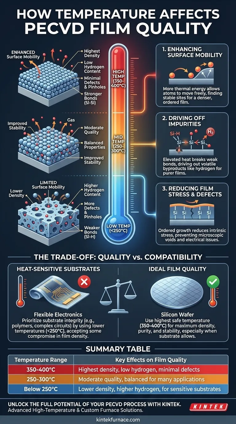
The Fundamental Role of Temperature in Deposition
While plasma provides the primary energy to initiate the chemical reaction in PECVD, substrate temperature plays a critical secondary role in determining the final structure and purity of the film.
Enhancing Surface Mobility
Higher temperature gives atoms and molecular fragments arriving at the substrate surface (known as adatoms) more thermal energy.
This increased energy allows them to move around more freely on the surface before locking into place. This process, called surface mobility, enables them to find more stable, lower-energy sites in the film's growing structure.
The result is a denser, more ordered film with a lower concentration of voids and structural defects.
Driving Off Impurities
PECVD precursor gases often contain hydrogen. During deposition, this hydrogen can become incorporated into the film, creating weak bonds (e.g., Si-H instead of Si-Si in silicon nitride) that degrade the film's chemical and mechanical stability.
Elevated temperatures provide the energy needed to break these weaker bonds and drive out volatile byproducts like hydrogen gas, leading to a purer, more stable final film. This is directly measured by a lower etch rate in subsequent processing steps.
Reducing Film Stress and Defects
The combination of higher surface mobility and impurity removal directly leads to films with lower intrinsic stress.
As the film grows in a more ordered and relaxed state, it is less prone to forming microscopic voids or pinholes, which are common defects in lower-temperature depositions that can compromise a device's electrical integrity.
Understanding the Trade-offs: Quality vs. Compatibility
The decision to use a higher temperature is not always straightforward. The primary reason for PECVD's existence is its ability to deposit films on materials that cannot survive the extreme heat of traditional thermal CVD processes.
The Core Advantage of PECVD
Conventional CVD can require temperatures approaching 1,000°C, which would melt, degrade, or fundamentally alter many important materials.
PECVD uses plasma to circumvent this thermal requirement, enabling deposition in a much lower range (from under 200°C to around 400°C). This capability is what makes modern microelectronics possible.
Protecting Heat-Sensitive Substrates
Many advanced applications rely on substrates that have strict thermal budgets. Materials like polymers for flexible electronics, certain metal layers in complex integrated circuits, or fully fabricated devices cannot withstand high temperatures.
In these cases, the maximum process temperature is dictated by the substrate's survival, not by the ideal conditions for the film itself.
The "Good Enough" Principle
A film deposited at 200°C will likely have more hydrogen and be less dense than one deposited at 400°C. However, that film is infinitely better than a melted substrate.
The goal is to find the highest temperature the substrate can tolerate to get the best possible film under those constraints. A film that is functional for the application is the real objective.
Making the Right Choice for Your Application
Optimizing temperature is a function of your end goal. There is no single "best" temperature, only the most appropriate one for your specific materials and performance targets.
- If your primary focus is maximum film quality and density: Use the highest temperature your substrate and equipment can safely and reliably handle, often in the 350-400°C range, to achieve the most stable and pure film.
- If your primary focus is depositing on a heat-sensitive substrate: Prioritize the integrity of your substrate by using a lower temperature (e.g., below 250°C), and accept the inherent trade-off in film density and purity.
- If your primary focus is balancing performance and process time: Begin in a mid-range (250-300°C) and characterize the resulting film, adjusting the temperature up or down to find the optimal point where film quality meets your device requirements without excessive thermal budget.
Ultimately, mastering PECVD temperature is about making a deliberate and informed choice based on the fundamental physics of film growth and the practical limits of your project.
Summary Table:
| Temperature Range | Key Effects on Film Quality |
|---|---|
| 350-400°C | Highest density, low hydrogen, minimal defects |
| 250-300°C | Moderate quality, balanced for many applications |
| Below 250°C | Lower density, higher hydrogen, for sensitive substrates |
Unlock the Full Potential of Your PECVD Process with KINTEK
Struggling to balance film quality with substrate thermal limits? KINTEK specializes in advanced high-temperature furnace solutions, including our CVD/PECVD Systems, designed to help you achieve superior thin films. Leveraging exceptional R&D and in-house manufacturing, we offer deep customization to precisely meet your unique experimental needs—whether you're working with heat-sensitive materials or aiming for maximum film density. Our product line, featuring Muffle, Tube, Rotary Furnaces, and Vacuum & Atmosphere Furnaces, ensures reliable performance and enhanced efficiency in your lab.
Don't let temperature compromises hold back your research—contact us today to discuss how KINTEK can tailor a solution for your specific application!
Visual Guide
Related Products
- Slide PECVD Tube Furnace with Liquid Gasifier PECVD Machine
- RF PECVD System Radio Frequency Plasma Enhanced Chemical Vapor Deposition
- Inclined Rotary Plasma Enhanced Chemical Deposition PECVD Tube Furnace Machine
- Inclined Rotary Plasma Enhanced Chemical Deposition PECVD Tube Furnace Machine
- Multi Heating Zones CVD Tube Furnace Machine for Chemical Vapor Deposition Equipment
People Also Ask
- What role does a Tube Furnace play in the CVD growth of carbon nanotubes? Achieve High-Purity CNT Synthesis
- In which industries is the tube furnace commonly used? Essential for Materials Science, Energy, and More
- What plasma source is used in PE-CVD tube furnaces? Unlock Low-Temperature, High-Quality Deposition
- What is plasma in the context of PECVD? Unlock Low-Temperature Thin Film Deposition
- What are the disadvantages of tube furnace cracking when processing heavy raw materials? Avoid Costly Downtime and Inefficiency


