In the semiconductor industry, Microwave Plasma Chemical Vapor Deposition (MPCVD) is a specialized process prized for creating high-purity, single-crystal diamond. This enables the fabrication of next-generation electronic devices that offer unparalleled performance in high-power and high-frequency applications by leveraging diamond's exceptional thermal and electrical properties.
As semiconductor devices become smaller and more powerful, managing heat and electrical stress becomes a primary bottleneck. MPCVD directly addresses this by making it possible to integrate diamond—the ultimate thermal conductor and a superior semiconductor material—into electronic systems, pushing performance far beyond the limits of silicon.
The Foundation: Deposition in Chip Manufacturing
What is Chemical Vapor Deposition (CVD)?
Chemical Vapor Deposition (CVD) is a foundational process in semiconductor manufacturing. It involves depositing extremely thin films of solid material onto a substrate, or wafer, from a gaseous state.
These films form the essential building blocks of an integrated circuit (IC), creating the insulating, conductive, and semiconducting layers that define a chip's function. The quality and uniformity of these films are critical for the device's final performance and reliability.
The CVD Family: Different Tools for Different Jobs
The term "CVD" covers a family of technologies. Standard CVD uses heat to drive the chemical reactions needed for deposition.
Another common method is Plasma-Enhanced CVD (PECVD), which uses a plasma to energize the gas molecules. This allows high-quality films to be deposited at much lower temperatures, which is crucial for building complex, multi-layered chips where high heat could damage existing structures.
MPCVD: Precision for Extreme Performance
How MPCVD Works
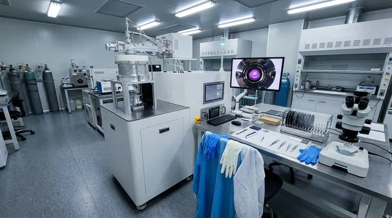
MPCVD is a more advanced form of CVD. It uses microwaves to generate a dense, highly controlled plasma in a vacuum chamber.
This high-density plasma allows for the growth of materials with exceptionally high crystal quality and purity, which is difficult to achieve with other methods. The primary application where MPCVD excels is the synthesis of single-crystal diamond.
The Diamond Advantage in Semiconductors
Silicon has been the workhorse of the industry for decades, but it has physical limitations. Diamond offers a suite of properties that make it a game-changing material for high-demand applications.
- Exceptional Thermal Conductivity: Diamond conducts heat more effectively than any other known material. When used as a substrate, it acts as a superior "heat spreader," pulling damaging heat away from the active components of a chip.
- High Breakdown Field: Diamond can withstand much stronger electric fields than silicon before breaking down. This allows for the creation of components that can handle significantly higher voltages without failing.
- Superior Carrier Mobility: Electrons and holes can move through the diamond lattice with very high velocity, enabling transistors that can switch on and off at much higher frequencies.
Where MPCVD Delivers Unique Value
The combination of these properties unlocks new levels of performance. MPCVD is essential for fabricating devices where performance is paramount.
This includes high-power transistors for 5G base stations and advanced radar systems, as well as ultra-efficient power electronics for electric vehicles and data centers. By reducing energy loss as heat, these diamond-based devices are not only more powerful but also more efficient.
Understanding the Trade-offs
High Cost and Lower Throughput
Growing high-quality, single-crystal diamond with MPCVD is a slower and more expensive process compared to depositing standard films like silicon dioxide with PECVD.
The equipment is complex, and the process requires precise control over long periods. This makes it economically viable only for applications where the performance benefits justify the added cost.
A Specialized Tool, Not a Universal Solution
MPCVD is not a replacement for general-purpose CVD or PECVD. Those methods remain the industry standard for depositing the vast majority of insulating and polysilicon layers in everyday electronics like phones and computers.
MPCVD is best understood as a specialized tool used to solve a specific, critical problem: overcoming the thermal and electrical limits of conventional semiconductor materials in the most demanding applications.
Making the Right Choice for Your Goal
When selecting a deposition technology, the goal dictates the tool.
- If your primary focus is extreme performance and power handling: MPCVD is the key to leveraging materials like diamond for next-generation, high-frequency devices where managing heat and voltage is the main challenge.
- If your primary focus is cost-effective, large-scale production: Standard thermal CVD and PECVD remain the essential workhorses for depositing the foundational layers in most integrated circuits.
- If your primary focus is depositing on temperature-sensitive layers: PECVD is the indispensable choice for building modern, complex chips without damaging previously fabricated structures.
Ultimately, mastering the right deposition technology for the right layer is fundamental to advancing the frontier of semiconductor innovation.
Summary Table:
| Feature | MPCVD | PECVD | Standard CVD |
|---|---|---|---|
| Primary Use | High-purity single-crystal diamond | Low-temperature film deposition | General-purpose film deposition |
| Key Advantage | Extreme thermal/electrical performance | Protects temperature-sensitive layers | Cost-effective for large-scale production |
| Ideal For | High-power/frequency devices (e.g., 5G, EVs) | Complex, multi-layered chips | Foundational layers in standard ICs |
Push the Limits of Semiconductor Performance with KINTEK
Is your R&D focused on overcoming the thermal and electrical bottlenecks of next-generation devices? MPCVD technology is critical for integrating high-purity diamond to achieve unparalleled performance in high-power and high-frequency applications.
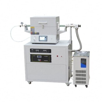
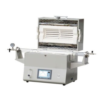
At KINTEK, we leverage our exceptional R&D and in-house manufacturing to provide advanced, high-temperature furnace solutions. Our product line, including specialized Tube Furnaces, Vacuum & Atmosphere Furnaces, and CVD/PECVD Systems, is complemented by strong deep customization capabilities to precisely meet your unique experimental requirements for materials like diamond.
Let's discuss how our MPCVD solutions can accelerate your semiconductor innovation.
Contact our experts today to explore a custom solution
Visual Guide

Related Products
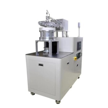
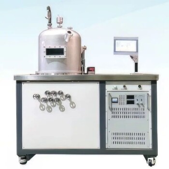
- MPCVD Machine System Reactor Bell-jar Resonator for Lab and Diamond Growth
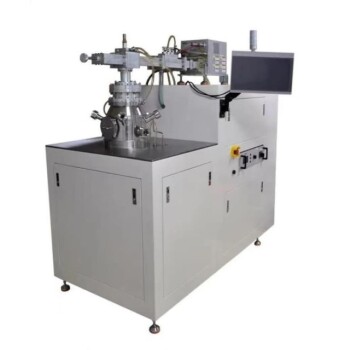
- Cylindrical Resonator MPCVD Machine System for Lab Diamond Growth
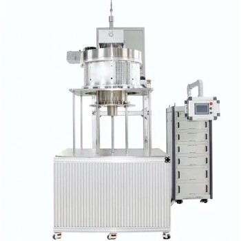
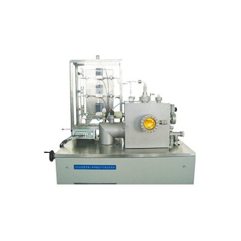
- 915MHz MPCVD Diamond Machine Microwave Plasma Chemical Vapor Deposition System Reactor
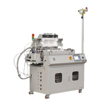
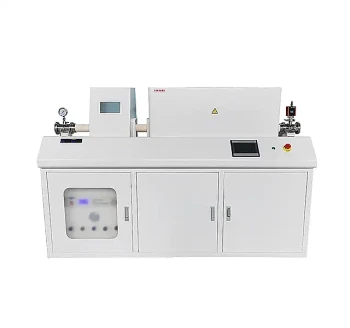
- Multi Heating Zones CVD Tube Furnace Machine for Chemical Vapor Deposition Equipment
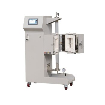
- Custom Made Versatile CVD Tube Furnace Chemical Vapor Deposition CVD Equipment Machine
People Also Ask
- What information does laboratory XRD provide for Gallium Sulfide? Master GaS Single Crystal Characterization
- What is the basic principle of operation for the microwave plasma chemical vapor deposition system? Unlock High-Purity Material Growth
- What is the function of injecting water in wood thermal modification? Unlock Superior Stability and Hydrophobicity
- How does MPCVD compare to other CVD methods like HFCVD and plasma torch? Uncover Superior Film Purity and Uniformity
- What advantages does the Laser Chemical Vapor Deposition (LCVD) process offer? High Purity & Precision SiC Fibers
