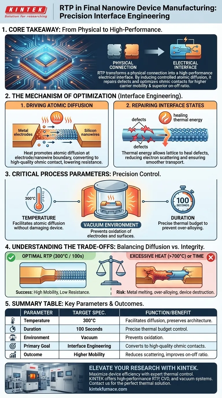
Rapid Thermal Processing (RTP) functions as a precise finishing step by subjecting the completed device to a vacuum anneal at 300°C for exactly 100 seconds. This controlled thermal burst serves to finalize the electrical integration of the device, specifically targeting the connection points between the metal electrodes and the nanowires.
Core Takeaway RTP transforms a physical connection into a high-performance electrical interface. By inducing controlled atomic diffusion, it repairs fabrication defects and optimizes ohmic contacts, directly resulting in higher carrier mobility and a superior on-off ratio for the transistor.
The Mechanism of Optimization
The primary goal of RTP in the final stages is not material synthesis, but interface engineering.
Driving Atomic Diffusion
The process uses heat to promote atomic diffusion at the boundary where the metal electrodes meet the silicon nanowires.
This diffusion lowers the resistance at the junction, converting the interface into a high-quality ohmic contact. Without this step, the barrier to electron flow would be too high, severely limiting device performance.
Repairing Interface States
Fabrication processes often leave behind structural defects or "interface states" on the nanowire surface.
The RTP cycle acts as a healing mechanism. The thermal energy allows the lattice to settle and repair these states, reducing electron scattering and ensuring smoother carrier transport.
Critical Process Parameters
Precision is the defining characteristic of this stage. Unlike bulk furnace annealing, RTP provides rapid heating and cooling rates to manage the "thermal budget."
Temperature and Time Constraints
The standard protocol for the final stage is a 300°C anneal for 100 seconds.
This specific window is critical; it provides enough energy to improve the contact but is short and cool enough to prevent unwanted diffusion or damage to other device layers.
The Role of Vacuum Environment
Performing this anneal in a vacuum is essential.
A vacuum environment prevents the oxidation of the metal electrodes and the nanowire surface during heating, ensuring that the improvements in conductivity are not negated by the formation of insulating oxide layers.
Understanding the Trade-offs
While RTP is a versatile tool capable of reaching much higher temperatures, applying it correctly in the final stage requires restraint.
High-Temperature Risks
RTP systems are capable of temperatures exceeding 700°C, often used in earlier stages for crystallizing materials like MoS2 or driving dopants.
However, utilizing such high temperatures on a completed device would be catastrophic. Excessive heat at the final stage could cause metal electrodes to melt, diffuse entirely into the nanowire, or degrade the delicate device architecture.
Balancing Diffusion vs. Integrity
The success of the process relies on a delicate balance.
Insufficient time or temperature results in poor contact resistance (Schottky barriers). Conversely, exceeding the 300°C / 100s limit risks over-alloying the metal with the semiconductor, physically consuming the nanowire and destroying the device.
Making the Right Choice for Your Goal
To maximize the efficacy of RTP in nanowire device fabrication, tailor your parameters to the specific stage of development.
- If your primary focus is Electrical Efficiency: Ensure the anneal reaches the full 300°C to guarantee sufficient atomic diffusion for low-resistance ohmic contacts.
- If your primary focus is Device Reliability: Strictly adhere to the 100-second duration limit to prevent thermal stress or over-diffusion that compromises the physical structure.
Summary: The RTP phase is the bridge between a fabricated structure and a functional electronic device, leveraging precise thermal control to unlock the full potential of carrier mobility.
Summary Table:
| Process Parameter | Target Specification | Function/Benefit |
|---|---|---|
| Temperature | 300°C | Facilitates atomic diffusion without damaging device architecture |
| Duration | 100 Seconds | Precise thermal budget control to prevent over-alloying |
| Environment | Vacuum | Prevents oxidation of electrodes and nanowire surfaces |
| Primary Goal | Interface Engineering | Converts junctions into high-quality ohmic contacts |
| Outcome | Higher Mobility | Reduces electron scattering and improves on-off ratios |
Elevate Your Nanowire Research with KINTEK
Maximize your device efficiency with precision thermal control. Backed by expert R&D and world-class manufacturing, KINTEK offers high-performance RTP, CVD, and vacuum systems designed for the most demanding lab requirements. Whether you are optimizing ohmic contacts or exploring new material boundaries, our customizable high-temperature furnaces provide the reliability you need.
Ready to refine your fabrication process? Contact KINTEK experts today to find the perfect thermal solution for your lab.
Visual Guide
References
- Lei Wu, Linwei Yu. Step-necking growth of silicon nanowire channels for high performance field effect transistors. DOI: 10.1038/s41467-025-56376-x
This article is also based on technical information from Kintek Furnace Knowledge Base .
Related Products
- Laboratory Quartz Tube Furnace RTP Heating Tubular Furnace
- RF PECVD System Radio Frequency Plasma Enhanced Chemical Vapor Deposition
- Split Multi Heating Zone Rotary Tube Furnace Rotating Tube Furnace
- Inclined Rotary Plasma Enhanced Chemical Deposition PECVD Tube Furnace Machine
People Also Ask
- What physical conditions does a laboratory Tube Furnace provide for SOEC? Precision Heat for Solid Oxide Characterization
- Why is a laboratory tube furnace necessary for BiVO4/RGO synthesis? Achieve Precise Nano-Structure Control
- What conditions do tube furnaces provide for Au-Seeded TiO2 nanowires? Master Precision Thermal Synthesis
- Why use multi-stage temperature control for REBCO pyrolysis? Prevent 75% Shrinkage Cracks and Ensure Film Density
- What conditions does a tube furnace provide for post-ion-implantation? Achieve Precise Microstructural Repair


